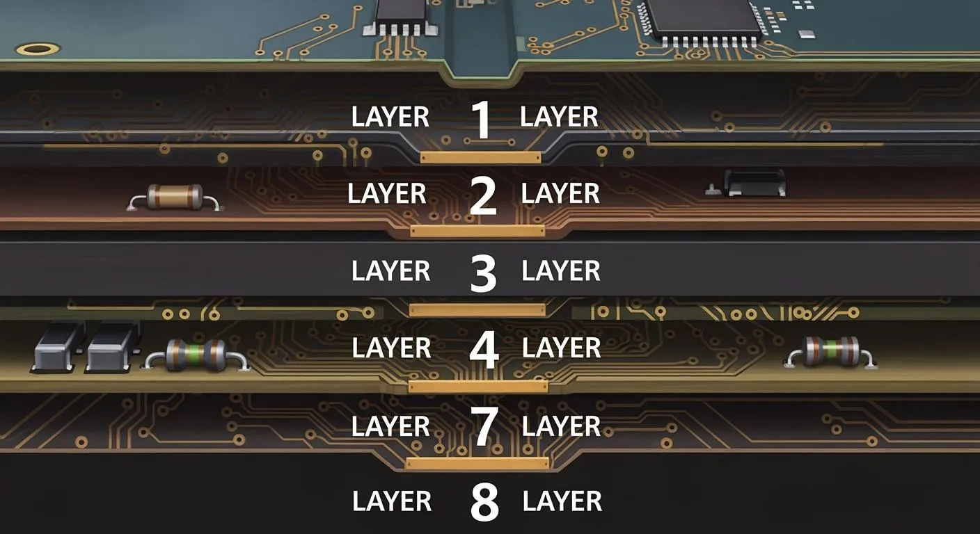
You might see that most pcbs have an even number of layers. Manufacturers pick an even number for making, working, and lasting reasons. This is not a hard rule, but it is now common. Odd-layer pcbs are out there, but you do not see them much. When you check normal pcb designs, you often see these layer numbers:
4 layers
6 layers
8 layers
Fancy devices sometimes use 18 to 30 layers, always with an even number. These choices help your electronic projects work better.
Key Takeaways
PCBs with even layers stay balanced. This helps stop bending and stress when making them. Picking even layers makes building PCBs faster. It also makes them cost less. Designs that are the same on both sides help signals move better. This means signals travel smoothly and have less noise. PCBs with odd layers are not used much. They are harder to make and cost more money. If you want strong and good PCBs, use an even number of layers.
Symmetry in Multilayer Printed Circuit Boards
Even Number of Layers and Material Balance
When you make multilayer printed circuit boards, you want the materials to be balanced. Using an even number of layers helps keep things even. Each layer matches with another layer on the other side. This makes a mirror image from the middle of the board. The board spreads out stress and heat in a fair way.
Symmetrical stackups help stop warping and stress. The board grows and shrinks the same on both sides.
You make the board stronger against heat and shaking. The board can handle changes in temperature and movement better.
You get steady results when making the board. Symmetrical designs help you avoid mistakes and problems.
If you use an odd number of layers, you lose balance. The board may not grow the same way everywhere. You might see more trouble when making the board. Most manufacturers pick an even number of layers for this reason. You get a tougher and more trustworthy pcb.
Tip: Always count your layers when planning multilayer printed circuit boards. A balanced stackup gives you better results and fewer problems.
Warpage and Structural Stability
Warpage is a big issue in multilayer printed circuit boards. It means the board bends or twists instead of staying flat. You want your pcb to stay straight and strong. Symmetry helps with this.
Asymmetrical layouts can make the board bend, twist, or get uneven. These problems make the board hard to use and can lower how well it works.
Warpage happens when the board is not balanced. Stress builds up in some spots, and the board bends.
An asymmetric setup can cause more stress in one place. This can make the board change shape or even break.
Even-numbered layers help the board stay flat. Studies show these boards usually bend less than 0.7%. Odd-layer boards, especially big ones, often bend more than 0.7%. This happens because the tension is not the same on both sides.
When you make a pcb, you press and heat the layers together. If you do not control this step, you can get layers that come apart, resin gaps, or layers that do not match up. These problems can make the board break early. Adding more layers makes these risks higher. That is why learning about lamination and symmetry is so important for multilayer printed circuit boards.
Note: A symmetrical design in multilayer printed circuit boards gives you better strength and helps your projects last longer.
Manufacturing Efficiency in PCBs
Streamlined Production with Even Layers
When you choose even layers for your pcb, you make the manufacturing process much easier. You avoid many problems that come with odd numbers of layers. Even-layer pcbs have a balanced structure. This balance helps you keep the board flat and strong during production. You do not need special design steps or extra work to fix bending issues. You save time and effort.
Even-layer pcbs reduce the risk of bending as the board gets thicker.
You get better quality control and faster production.
Balanced lamination keeps your pcb strong and prevents warping.
You spend less money because you avoid extra steps and repairs.
If you pick a 3 layers pcb, you face more challenges. You need special design arrangements. These steps take more time and increase your workload. Odd-layer pcbs often bend because the tension is not the same on both sides. You may see higher costs and more mistakes. When you use a 4 layers pcb, you get a smoother process. Manufacturers can make these boards quickly and with fewer problems.
Multi-layer pcbs with even layers help you keep production efficient. You do not waste time fixing errors or dealing with warped boards. You get a reliable product that meets your needs.
Tip: If you want to save time and money, choose even layers for your pcb design. You will see better results and fewer headaches.
Error Reduction and Yield Improvement
You want your pcb to work well and last long. Even-layer pcbs help you reach this goal. They lower the chance of errors during manufacturing. You get higher yields, which means more good boards and less waste.
Here is a table that shows how error rates and efficiency compare between even-layer and odd-layer designs:
Design Type | Error Rate Impact | Manufacturing Efficiency |
|---|---|---|
Even-layer | Lower error rates | Higher efficiency |
Odd-layer | Higher error rates | Lower efficiency |
When you use a 3 layers pcb, you see more mistakes. The board may warp or fail quality checks. You spend more time fixing problems. Odd-layer pcbs need special processes, which slow down production and raise costs. You also use more labor and materials, which hurts your budget.
Multi-layer pcbs with even layers offer better interference resistance. The copper foil and substrate stay at stable distances. This setup helps your signals move faster and with less delay. You get a board that works better and lasts longer.
If you want to improve your yield and reduce errors, stick with even layers in your pcb design. You will see more reliable boards and happier customers.
Note: Choosing even layers for your multi-layer pcbs helps you avoid costly mistakes and keeps your production line running smoothly.
Signal Integrity and Performance
Equal Signal Access Across Layers
You want signals to move easily in your multilayer pcb. Using an even number of layers makes the board balanced. This helps each signal layer reach ground and power planes the same way. You do not get uneven signal paths. The stack-up stays symmetrical, so signals move at the same speed on both sides.
A symmetrical stack-up in multilayer pcbs gives you many good things:
You keep the dielectric thickness and copper spread the same. This means signal layers have steady impedance, which is needed for high-speed signals.
You cut down on crosstalk. Ground planes sit next to signal layers in a balanced way. This shields each signal layer and keeps signals clean.
You lower electromagnetic interference. Signals follow a steady return path, so your pcb works better for high-frequency designs.
When you design a multi-layer pcb, you want every signal to get where it should go without loss or delay. A balanced structure helps you do this. You get good performance and fewer signal problems.
Tip: Always check your stack-up for symmetry. Balanced multilayer pcbs help signals stay strong and clear.
Controlled Impedance in PCB Design
Impedance control is important in multilayer pcb design. You need to keep impedance steady across all layers. Using an even number of layers makes this easier. The structure stays balanced, and the stack-up supports steady signal flow.
Here are some main points about impedance and signal loss in multilayer pcbs:
Trace width changes single-ended and differential impedance. You must adjust trace spacing and substrate thickness to keep impedance steady.
The highest crosstalk coefficient changes with trace spacing. Good design choices help you lower crosstalk and signal loss.
Electrostatic capacitance in differential wiring drops in slit sections compared to solid planes. This affects crosstalk levels in your pcb.
A symmetrical stack-up lets you control impedance better. You keep copper and dielectric thickness even across all layers. Your multi-layer pcb works well for high-speed signals and tough circuits. You avoid signal loss and keep your board working well.
Note: Controlled impedance in multilayer pcbs helps you build strong, high-performance electronic devices.
Odd-Layer PCBs and Their Challenges

Manufacturing Issues with Odd Layers
If you use odd-numbered layer pcbs, you face many problems. You need to be careful with alignment. If holes and vias do not line up, your pcb may fail. Odd-number multilayer printed circuit board designs can bend or twist. These issues make your board hard to use.
Here is a table that shows the main problems:
Challenge | Description |
|---|---|
You must line up holes and vias just right. Mistakes can cause current flow problems and bending. | |
Increased Fabrication Cost | You spend more money on materials and work. More layers mean higher costs. |
Difficult Repair | If you find mistakes inside, you cannot fix them easily. Repairs are almost impossible. |
Odd-numbered layer pcbs also have more defects. You need special bonding steps. These steps slow down how fast you can make boards. It is harder to keep the board flat, especially for big pcbs. You may not meet IPC600 rules for flatness.
Note: Odd-number multilayer printed circuit board designs need extra steps. These steps take more time and cost more.
Why Odd-Layer PCBs Are Rare
You do not see odd-layer pcbs in most products. Manufacturers stay away from them for many reasons. Odd-layer designs cost more to make. You need special lamination steps. These steps can cause more mistakes and bending. You also lose assembly speed. Special tools and steps slow down making boards.
Here is a table that compares odd-layer and even-layer pcbs:
PCB Type | Cost of Manufacturing | Design Complexity | Frequency of Use |
|---|---|---|---|
Odd-layer | More expensive | Complicated | Less frequent |
Even-layer | Cost-effective | Easier | More frequent |
Most manufacturers want a balanced stack-up. Even-layer designs give better strength and easier making. Odd-layer pcbs are used in special cases. Wearable devices, medical implants, and car sensors sometimes use odd-number multilayer printed circuit board designs. These boards need special shapes or weight limits.
Tip: If you want a strong pcb, pick a balanced stack-up with an even number of layers. You will save money and get better results.
You should pick an even number of layers for your printed circuit board. This helps your board stay balanced and work well. Most manufacturers say this is the best way. It stops the board from bending and saves money by avoiding mistakes. Odd-layer PCBs do exist, but they cost more and are harder to design. You do not see them often. When you plan your next printed circuit board, think about space and power needs. Also, think about any changes you might need later. Always try to make your pcb strong and work well every time.
FAQ
Why do you rarely see odd-layer PCBs?
You rarely see odd-layer PCBs because they bend more easily. Manufacturers find them harder to make. You also pay more for them. Most companies choose even layers for better strength and lower cost.
Can you use an odd number of layers if you want?
You can use an odd number of layers, but you will face more problems. Your board may warp or fail tests. Most experts suggest you use even layers for better results.
What is the most common number of layers in PCBs?
You often see 2, 4, 6, or 8 layers in PCBs. Four-layer and six-layer boards are very popular. You pick the number based on your circuit’s needs.
Does more layers mean better performance?
More layers can help with complex circuits. You get better signal control and less interference. You should only add layers if your design needs them.
How do you count PCB layers?
You count each copper layer in your PCB. For example, a four-layer PCB has four copper sheets. You include both signal and power layers in your count.