You have special problems when you work with optical communication equipment. Sending data very fast means you must be careful with every part of PCB Design. You must connect optical modules and electronic parts while thinking about fast data.
Being exact and making sure things work well is most important.
Using better inspection helps you find small mistakes before they turn into big trouble.
Working with photonics technologies helps you get faster and steadier connections.
Key Takeaways
Focus on keeping high-speed signals clear in PCB design. This helps stop problems like signal reflections and crosstalk. It makes sure data moves correctly and without mistakes.
Use controlled impedance and the right layer stackup for good signals. Matching trace impedance stops signal bounce and errors.
Use good thermal management to stop overheating. Spreading heat well keeps optical modules working right. It also helps them last longer.
Pick low-loss dielectric materials for stronger and faster signals. These materials lower energy loss and help high-frequency work better.
Test and check quality often to make sure things work well. Regular checks and following rules keep optical communication systems working great.
PCB Design Requirements
High-Speed Signal Integrity
When you work with optical communication equipment, you need to watch high-speed signal integrity. High-speed signals move very quickly, sometimes faster than 10GHz. Even small mistakes in pcb design can cause big problems at these speeds. You have to make sure signals get to the right place at the same time and keep their shape. If you do not, you might see reflections, crosstalk, or electromagnetic interference (EMI).
High-speed pcb design needs careful routing so signals do not get lost.
Impedance mismatches can make signals bounce back and cause errors.
Crosstalk can put extra signals in your data and make it worse.
Power changes can also mess up signal integrity.
You should use smaller microvias and high-density interconnect (HDI) pcb technology to stop breaks in the path. Try to keep trace stub lengths short. Differential signaling and tightly coupled pairs help keep signals safe from outside noise. If you do not control these things, you might see signals get weaker, less bandwidth, and more mistakes.
Controlled Impedance & Layer Stackup
Controlled impedance is very important for high-speed pcb design. You need to match the impedance of traces to the parts they connect. If you do not, signals can bounce back and cause mistakes. Layer stackup is how you put the layers inside your pcb. A good stackup helps control impedance and keeps noise down.
Use the right materials and trace widths for your pcb design.
Put ground and power planes close to signal layers.
Keep high-speed signals on inside layers if you can.
You should plan your pcb stackup early when you start designing. This helps you stop problems before they happen. Good impedance control keeps your high-speed signals clean and working well.
Crosstalk, EMI, and Shielding
Crosstalk and EMI can hurt your high-speed pcb design. Crosstalk happens when signals from one trace jump to another. EMI is noise from electronic parts that can move through the air or the pcb. You need to use shielding to keep your signals safe.
Shielding Technique | Description |
|---|---|
Metal enclosures or cans | Cover whole pcb parts or delicate components to lower EMI. |
Grounding strips | Wide copper strips around noisy areas help stop EMI radiation. |
You should keep high-speed traces far apart and use ground planes to block noise. Shielding helps keep your pcb design safe from outside signals. This is very important for optical communication equipment.
Thermal Management in PCB Design
High-speed optical modules can get hot. Good thermal management in pcb design keeps your equipment working well. If you do not control heat, you might see lower signal quality, more mistakes, or even broken devices.
Put hot parts apart to spread out heat.
Use copper planes to move heat away from parts.
Add thermal pads and underfill to help heat move to the board or heatsink.
Use thermal vias under hot parts to send heat to other layers.
Try embedded copper coins or vapor chambers for very hot spots.
If you do not manage heat, you might see problems like weaker signals, more mistakes, faster wear, or even total failure.
Tip: Always check your pcb design for hot spots before you finish. Good thermal management helps your high-speed optical equipment last longer.
Material Selection for Optical PCBs
Low-Loss Dielectrics
You need to pick the best materials for your optical pcb. Low-loss dielectrics help signals stay strong and clear. These materials stop energy from turning into heat. When you use low-loss dielectrics, your high-frequency pcb sends data faster and with fewer errors. Here are some common low-loss dielectric materials used in bare board fabrication for optical equipment:
Fluorinated polymers like PTFE and PFCB
Polyimides (PI)
Polyphenylene ethers (PPE)
Polybenzoxazoles (PBO)
Boron nitride (BN)
N4000-13
You want materials with a low dissipation factor and a low dielectric constant. These things help your pcb keep signals strong, even at high speeds. Check the table below to see why these things matter:
Property | Description |
|---|---|
Dissipation Factor | Shows how much energy turns into heat. Lower is better for optical signals. |
Dielectric Constant | Tells how well the material holds electric energy. Lower is better for speed. |
High-Frequency Laminates
High-frequency laminates are important in bare board fabrication for optical communication. You need these laminates to keep signals moving fast and without loss. Materials like PTFE and ceramic-filled laminates work well for this. You might also use Rogers RO3003 or Isola I-Speed. These laminates have a low dielectric constant and a low dissipation factor. This means your pcb will lose less signal and keep signal integrity better. You can trust these materials to keep your optical data moving quickly and safely.
The dielectric constant affects how fast signals move.
The dissipation factor shows how much signal turns into heat.
Good laminates help your pcb keep up with optical network needs.
Compatibility with Optical Components
You must make sure your pcb materials work well with optical components. Many optical systems use silicon because it is clear at 1550 nm, which matches most optical fiber networks. Sometimes, you need to bond special semiconductors to silicon to add light sources or detectors. This can make bare board fabrication harder. You also need to think about power and heat. High-power optical modules need materials that can handle heat. Low-power modules need materials that are sensitive enough for weak signals.
Material compatibility keeps your optical alignment steady.
Good mechanical stability helps your optical modules last longer.
Thermal management is important because optical parts can get hot.
The right adhesives and encapsulants protect your pcb from the environment.
Tip: Always check that your pcb materials match your optical components before you start bare board fabrication. This helps you avoid problems and keeps your optical equipment working well for a long time.
PCB Manufacturing Requirements
Precision Fabrication & Tolerances
You have to be very careful when making pcbs for optical communication equipment. High-speed signals need paths and connections that are just right. Even tiny mistakes can cause big problems with signals and how well things work. You must follow strict rules for every step of making the pcb.
Here is a table that shows the standard tolerances you should meet during pcb fabrication:
Tolerance Type | Specification |
|---|---|
Drilled Holes | ±0.05 mm |
Trace Width and Spacing | ±0.05 mm to ±0.1 mm |
Board Dimensions | ±0.1 mm to ±0.2 mm |
Solder Mask Tolerances | Alignment with pads is critical |
Via Tolerances | Tighter tolerances for microvias |
You need to make sure drilled holes and vias are in the right spot. If you miss by a little, signals can get worse. You also have to control trace width and spacing. If you do not, signals can get lost or mixed up. The board must be the right thickness, or it might not fit or work.
Being exact when making pcbs helps you:
Keep layers lined up within ±0.05 mm. This stops vias from being off and keeps signals strong.
Put drill holes in the right place within ±0.075 mm. This keeps high-speed pcbs working well.
Control trace width and spacing to within ±10%. This lets you make dense pcbs without losing signals.
Keep board thickness within ±0.1 mm. This makes sure your pcb works with optical modules and other parts.
You must follow these rules every time you make a pcb. If you do not, you could lose signals, have weak boards, or your optical equipment could fail.
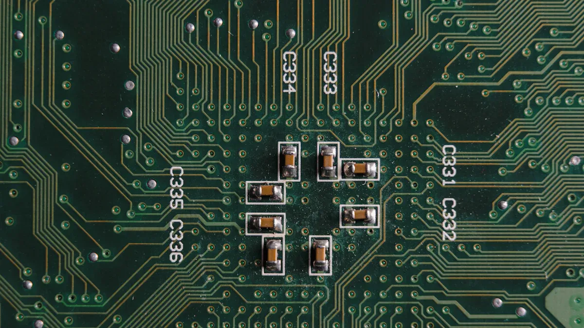
Optical Inspection & Layer Registration
You need special inspection tools when making pcbs for optical communication equipment. Inspection helps you find small problems before they get worse. You must check every layer of the pcb, not just the outside. Problems can hide inside and hurt how the pcb works.
Optical inspection tools help you see tiny problems in copper traces, vias, and solder masks. You can find things like bad alignment, shorts, or open spots early. You also need to check that all layers line up right. If they do not, you can get broken connections or weak signals.
You must keep layers lined up very closely. Many things can change how well layers line up:
Film can stretch from heat or wet air.
Punched holes in the film must be accurate.
Exposure systems must keep layers straight.
UV markers must be in the right spot for inner layers.
Holes must be in the right place.
Direct Imaging systems must line up layers well.
You need to use optical inspection at every step of making the pcb. This means checking inside layers, outside layers, and the final board. You should also use automated optical inspection (AOI) to check faster and find more problems. AOI uses cameras and computers to look for mistakes quicker than people.
Tip: Always look at your inspection results after each step. This helps you find mistakes early and fix them before they cost more.
Cleanroom Control & Surface Finishes
You must keep the area clean when making pcbs. Dust, oil, and other tiny things can ruin your pcb. Even a small speck can cause a short or break a connection. You need cleanrooms for the most important steps. Cleanrooms use special filters to keep dust and dirt out of the air.
You also need to control temperature and humidity. If these change, the pcb can bend or the film can stretch. This can mess up layer alignment and signal quality. You have to wear gloves and clean suits to keep oil and dirt off the pcb.
Surface finishes are also important for making pcbs for optical communication equipment. You need special finishes for high-speed and high-frequency signals. Some of the best finishes are ENIG and ENEPIG. These finishes give you:
Better soldering.
Stronger protection from rust.
Smooth surfaces for high-frequency signals.
Less signal loss in fast circuits.
Stronger solder joints that last longer.
You must pick the right finish for your pcb. ENIG and Immersion Silver are good for high-frequency pcbs. They help keep signals strong and make your equipment last longer.
Note: Always check your surface finish for problems during inspection. A good finish helps your pcb work well and last longer.
You must follow strict rules for keeping things clean, using good plating, and checking for problems at every step. This keeps your pcb safe, strong, and ready for fast optical communication.
Testing and Quality Assurance
Signal Performance Testing
You have to test each pcb and module. This makes sure your equipment works well. Signal performance testing checks if data moves without mistakes. You use tools like eye diagrams and bit error rate tests. These tests show if your signals are clear and strong. A clear eye diagram means good timing and little noise. Bit error rate testing finds mistakes in sending data. Error correction can help make things more reliable. Good signal testing helps your module work well outside and keeps communication steady.
Tip: Always test signal performance after you build your module. This helps you find problems before using the module.
Reliability & Environmental Testing
You need to check if your pcb and module can handle tough places. Reliability and environmental testing makes sure your module works in heat, shaking, and wet air. You use rules to guide your tests. Here is a table with some important standards for pcb reliability and environmental testing:
Standard Type | Description |
|---|---|
Military | MIL-STD-810 gives hard tests for heat, wet air, high places, shaking, and shocks. |
JEDEC | Checks how chips handle wet air and changing temperatures. |
Automotive | AEC-Q100 tests car electronics for heat and chemicals. |
International | IEC 60068 gives world rules for testing electronics in tough places. |
You run these tests on every module. This makes sure your pcb can work in real life. If your module passes, your equipment will last longer.
Compliance with Industry Standards
You must follow strict rules when you test your pcb and module. Industry standards help keep your module safe and strong. You use standards for fast communication and optical transmission. These rules tell you how to test and what results you need. When you follow these rules, your module works with other equipment and meets customer needs. You check every pcb and module for these rules before shipping. This keeps your system ready for fast communication.
Optical Module PCB Challenges
High-Density Interconnects & Miniaturization
Designing optical module pcbs is hard because you need to fit many data paths in a small space. High-density wiring lets you move more data quickly. You have to use special pcb materials to keep signals strong. You also need to think about how easy it is to make and put together the pcb. This helps make sure the pcb works well.
Here are some main problems with high-density interconnects:
You need materials that can handle more data in the future. Many photonic circuit materials are still being tested.
You must change how you make pcbs to work with optical interconnects.
You have to design good I/O interfaces for the optical module pcb. These help connect the data paths.
Miniaturization means making the pcb smaller. This lets you fit more parts and data in less space. You must keep the pcb reliable, even when it is tiny. You need to plan how to put parts on the pcb from the start.
Integration & Hot-Swapping
You need to connect many parts on the optical module pcb. Integration means putting photonic and electronic parts together. This helps you move data faster. You must use high-speed pcb design to keep data safe. You also need to plan how to build and fix the pcb. This makes assembly and repairs easier.
Hot-swapping lets you change the optical module pcb without turning off the system. You must design the pcb and parts to handle this. You need strong connectors and good assembly. This keeps data moving and helps the pcb last longer.
Tip: Always check if your design is easy to make and put together before you finish. This helps you avoid problems later.
Shielding and Separation of Components
You must keep noise away from the data on the optical module pcb. Shielding stops outside signals from hurting your data. You can use metal covers or ground planes on the pcb. You also need to keep fast parts away from other parts. This helps stop crosstalk and keeps data safe.
You must plan the layout for easy assembly and strong design. This helps the pcb stay reliable. Good shielding and separation make sure your optical module pcb works well in fast data systems.
Challenge | Solution Example |
|---|---|
Crosstalk | Use ground planes and spacing |
EMI | Add metal shields |
Assembly errors | Plan for design for assembly |
You always need to think about assembly, data, and reliability when you design an optical module pcb. This helps you build strong and fast systems.
You must focus on quality at every step of PCB design and manufacturing for optical communication equipment. Quality starts with your choice of materials. You select materials that support high-speed signals and keep quality high. You use advanced inspection to check every layer and every trace. Quality means you follow strict standards. You test your boards to meet these standards. You check quality with every inspection. You make sure your boards meet industry standards. You use quality control to catch problems early. You keep quality as your main goal. You use standards to guide your work. You check quality in every process. You use standards for testing. You keep quality in mind when you pick materials. You use standards for assembly. You use quality checks for every board. You use standards for inspection. You use quality to make your boards last longer. You use standards to keep your boards safe. You use quality to keep your signals strong. You use standards to help your boards work with other equipment. You use quality to make your boards reliable. You use standards to make sure your boards pass every test. You use quality to keep your boards working in tough places. You use standards to help your boards handle heat and vibration. You use quality to make your boards easy to assemble. You use standards to help your boards fit with optical modules. You use quality to keep your boards clean. You use standards to help your boards resist rust. You use quality to keep your boards safe from dust. You use standards to help your boards last longer. You use quality to keep your boards strong. You use standards to help your boards pass inspection. You use quality to keep your boards ready for fast data. You use standards to help your boards meet customer needs. You use quality to make your boards the best they can be. You use standards to guide every step. You use quality to make sure your boards work in high-speed optical networks.
FAQ
What materials work best for high-speed optical PCBs?
You should pick low-loss dielectrics like PTFE or ceramic-filled laminates. These materials help signals stay strong and stop mistakes. They also let data move fast in optical networks.
How do you prevent signal loss in PCB design?
You can use controlled impedance, short trace lengths, and differential pairs. Shielding and ground planes help too. These ways keep signals clear and cut down on noise.
Why is cleanroom control important during PCB manufacturing?
Cleanroom control keeps dust and oil off your PCB. Even a tiny bit of dirt can cause shorts or weak spots. You get better boards that last longer.
What tests should you run on optical communication PCBs?
You should run signal tests, reliability checks, and environmental tests. Use tools like eye diagrams and bit error rate testers. These tests show if your board works well in real life.
Can you use regular PCBs for optical modules?
Regular PCBs do not work well in high-speed optical systems. You need special materials, tighter rules, and better inspection. These things help your board handle fast data and tricky optical parts.