Selecting the right hybrid PCB materials plays a crucial role in achieving high performance and reliability while keeping costs in check. You should match material properties like coefficient of thermal expansion (CTE) to copper—ideally around 17 ppm/°C—to reduce thermal stress and prevent delamination.
Metric | Value | Impact |
|---|---|---|
Failure rate (sensors) | 2% | 20,000 defects per million units |
CTE of copper | ~17 ppm/°C | Reduces stress, improves reliability |
Frequency range | Up to 77 GHz | Needs stable, compatible materials |
Choosing compatible layers and following IPC guidelines helps you avoid costly failures and manufacturing issues in hybrid PCB production.
Key Takeaways
Choose hybrid PCB materials that match copper’s thermal expansion to reduce stress and prevent damage.
Consider electrical, thermal, and mechanical needs to ensure your PCB performs well and lasts longer.
Use simulation tools and testing to find and fix problems before manufacturing your PCB.
Work closely with your manufacturer early to improve design feasibility and avoid costly errors.
Balance cost and performance by using advanced materials only where needed and standard materials elsewhere.
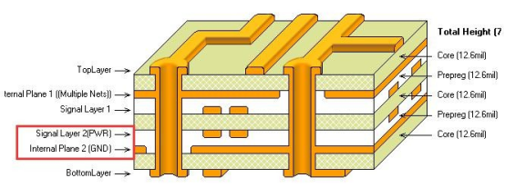
Hybrid PCB Overview
What Is a Hybrid PCB
You encounter hybrid PCBs in many advanced electronic systems. These circuit boards combine several types of pcb material and technologies within a single structure. Unlike traditional boards, you use hybrid pcb materials such as FR-4 fiberglass, ceramics, metal-core, polyimide, and PTFE to meet specific performance needs. This approach lets you optimize for signal integrity, thermal management, and mechanical stability.
Hybrid pcb materials support multilayer designs, including rigid-flex and high-frequency boards.
You find these boards in aerospace, automotive, medical, and consumer electronics.
Applications of hybrid pcb materials include communication systems, imaging devices, and high-speed computing.
Recent research highlights the shift from manual inspection to automated optical inspection (AOI) for hybrid PCBs. Deep learning and hybrid optical sensors now detect micro-size defects with high accuracy. These advances improve quality control and reduce errors before mass production.
Tip: When you select hybrid pcb materials, consider the application and the required performance for each layer.
Why Material Choice Matters
Your choice of pcb material directly affects the efficiency and reliability of your hybrid PCB. Each material brings unique electrical, thermal, and mechanical properties. For example, ceramic-based substrates offer excellent thermal dissipation, while polyimide provides flexibility for dynamic environments.
You must match the coefficient of thermal expansion (CTE) between copper and the substrate to prevent delamination.
Material selection impacts signal transmission, electromagnetic interference, and mechanical durability.
The right hybrid pcb materials reduce manufacturing defects and extend product life.
Empirical studies show that changes in material geometry, such as pad diameter, can reduce the thermal cycling life of assemblies by over 90%. Vibrational damage often occurs in the z-direction, so you should reinforce the board and optimize the stack-up. Advanced modeling techniques now help you predict how each pcb material will behave under stress, improving your design decisions.
Note: Always align your material choices with the application’s frequency, power, and environmental demands.
Hybrid PCB Materials

Electrical and Thermal Needs
When you select hybrid PCB materials, you must evaluate how each pcb material meets your electrical and thermal requirements. The right choice ensures your design supports high-speed signals, stable power delivery, and effective heat dissipation. You should always match the electrical performance of each layer to your application. For example, high-frequency circuits in radar or wireless devices need materials with low dielectric loss and stable dielectric constant. These characteristics help maintain signal integrity and reduce losses in high-speed design.
Thermal conductivity is another critical factor. You want your hybrid PCB to manage heat efficiently, especially in power electronics or densely packed assemblies. Studies show that using nano-enhanced phase change materials with Al2O3 nanoparticles in different heat sink configurations can reduce base temperatures by up to 36.2% at certain heat fluxes. This improvement in thermal management helps prevent overheating and extends the life of your device.
You should also consider the glass transition temperature (Tg) and coefficient of thermal expansion (CTE) when choosing pcb material. A Tg above your operating temperature ensures the substrate remains stable. Matching the CTE of your substrate to copper, which is about 17 ppm/°C, reduces the risk of delamination and mechanical stress during thermal cycling.
Tip: Always align the thermal conductivity and electrical performance of your hybrid PCB materials with the specific demands of your application.
Mechanical Properties
Mechanical durability is just as important as electrical and thermal performance. You need hybrid PCB materials that can withstand vibration, flexing, and repeated thermal cycles. Experimental studies have measured the elastic modulus, relaxation modulus, and creep compliance of materials like thermal conductive silica gel used in PCB packaging. These parameters help you predict how your hybrid PCB will behave under stress.
You can use simulation tools and artificial neural networks to estimate the mechanical properties of your hybrid PCB materials. For example, combining finite element analysis with experimental data has achieved a mean absolute percentage error of about 1.2% when predicting natural frequencies. This high level of accuracy gives you confidence in your material selection and stack-up design.
When you choose pcb material, look for characteristics such as high elastic modulus and good stress relaxation. These features improve the mechanical stability of your hybrid PCB, especially in demanding environments like automotive or aerospace applications. You should also consider the cushioning and creep behavior of encapsulants and adhesives, as these can affect the long-term reliability of your assembly.
Note: Mechanical properties are essential for applications of hybrid PCB materials in environments with frequent vibration or temperature changes.
Advanced Material Options
You have access to advanced hybrid PCB materials that offer unique benefits for specialized applications. Liquid Crystal Polymer (LCP) stands out for its high working temperature, excellent chemical resistance, and strong barrier properties. LCP prevents moisture ingress, which is a common cause of failure in polyimide-based devices. The monolithic fusing of LCP layers creates a hermetic seal, protecting wiring and extending device longevity.
LCP also supports standard flexible PCB manufacturing processes, making it compatible with existing production lines. You can thermoform LCP substrates into complex shapes, and they can operate at temperatures up to 190 °C. These material characteristics make LCP ideal for medical, aerospace, and miniaturized sensor modules. The low permeability to gases and water, combined with strong adhesion, ensures reliable performance in harsh environments.
Graphene is another emerging pcb material with exceptional electrical performance and thermal conductivity. Its unique structure allows for rapid electron movement, making it suitable for high-speed design and next-generation electronics. While still in the early stages of adoption, graphene-enhanced hybrid PCB materials promise significant improvements in both signal integrity and heat management.
Callout: Advanced hybrid PCB materials like LCP and graphene enable you to push the boundaries of performance, reliability, and miniaturization in your designs.
You should always evaluate the full range of material characteristics, including electrical performance, thermal conductivity, and mechanical durability, when selecting hybrid PCB materials for your next project.
Selection Criteria
Performance Factors
You need to evaluate several critical factors when selecting hybrid PCB materials. Electrical performance stands at the top of your list. You should check the dielectric constant (Dk) and dissipation factor (Df) for each pcb material. Low Dk and Df values help reduce signal loss, especially at high frequencies. Stability of these values across your frequency range ensures signal integrity. Copper foil surface roughness also affects conductor loss and skin effect, which can impact routing and overall electrical performance.
Thermal conductivity and the thermal coefficient of dielectric constant (TcDk) are important characteristics. These influence how your hybrid PCB manages heat and maintains circuit stability. Moisture absorption can degrade electrical performance, especially in humid environments. You should use multiphysics simulation tools to predict how your chosen materials will perform under real-world conditions. These tools help you optimize your design requirements and routing guidelines for high reliability.
Tip: Always compare electrical performance using experimental data under consistent test conditions, not just supplier specifications.
Cost Considerations
Cost plays a major role in your material selection process. Specialized hybrid PCB materials, such as high-frequency or high-temperature substrates, increase your material costs compared to standard pcb material like FR-4. The number of layers, copper thickness, and complexity of routing all add to your expenses. Advanced via types and tighter tolerances also raise manufacturing costs.
Cost Factor | Impact on Hybrid PCB Production Cost |
|---|---|
Material Selection | High-performance materials increase costs over standard pcb material. |
Layer Count | More layers mean higher material and processing costs. |
Surface Finish | Special finishes like immersion silver add to expenses. |
Routing Complexity | Complex routing and advanced vias require more time and resources. |
You can balance performance and cost by using high-frequency materials only on layers with critical signals and standard pcb material elsewhere. This approach meets your performance needs without over-designing and overspending.
Compatibility
Compatibility between different hybrid PCB materials is essential for a reliable product. You must match the coefficient of thermal expansion (CTE) between materials to prevent warpage and delamination. Incompatible materials can cause structural failures, especially during thermal cycling. You need to select bonding processes that ensure strong adhesion between layers.
Manufacturing hybrid PCB assemblies often requires specialized equipment and precise control over temperature, pressure, and time. These steps help you achieve reliable bonds and maintain the desired material characteristics. Following established guidelines and routing guidelines reduces the risk of compatibility issues and supports high reliability in your application.
Note: Always consider the full range of material characteristics and compatibility when designing your hybrid PCB for demanding environments.
Hybrid PCB Challenges
Material Compatibility
You face major challenges in hybrid pcb design when you combine different hybrid pcb materials. Each material has unique properties, such as coefficient of thermal expansion (CTE) and dielectric constant. If you do not match these properties, you risk delamination and poor electrical performance. Adhesive systems must bond well with every layer to keep the board strong over its entire life. You should always check the feasibility of your material choices before starting hybrid-board manufacturing. This step helps you avoid costly redesigns and failures.
Tip: Use simulation tools to predict how hybrid pcb materials will interact under heat and stress.
Warpage and Stress
Warpage and stress often appear during the manufacturing and operation of hybrid PCBs. When you use hybrid pcb materials with different CTEs, the board can bend or twist as it heats and cools. This movement puts stress on solder joints and can cause cracks or open circuits. Studies use finite element analysis (FEA) and thermal cycling tests to measure these effects. However, most tests report only pass or fail results. They do not give you detailed statistics about failure rates or the main causes of problems. This lack of data makes it hard to pinpoint the biggest challenges in hybrid pcb reliability.
FEA models show where stress builds up in solder joints.
Life tests use about 45 units per batch but do not separate failure mechanisms.
Ongoing research tries to improve statistical analysis for better reliability predictions.
You should always consider the feasibility of your design by reviewing both simulation and real-world test results.
Manufacturing Complexity
Hybrid pcb materials add complexity to the manufacturing process. You must control temperature, pressure, and timing for each material to avoid defects. Differences in CTE can cause mechanical stress and threaten the board’s structure. Electrical properties like impedance and crosstalk also change with each material’s thickness and surface roughness. You need compatible adhesives to prevent delamination between layers. Proper laminate selection and layer separation are key steps in hybrid-board manufacturing.
Manufacturing Issue | Impact on Feasibility and Reliability |
|---|---|
CTE mismatch | Increases warpage and stress |
Adhesive compatibility | Reduces delamination risk |
Electrical differences | Affects signal integrity and performance |
You must address these challenges in hybrid pcb production to ensure your final product meets quality and reliability standards.
Overcoming Challenges
Stack-Up Design
You can solve many hybrid PCB issues by focusing on stack-up design. Start by selecting materials with compatible coefficients of thermal expansion. This step reduces warpage and stress during temperature changes. Arrange your layers to separate high-speed signals from power planes. This approach improves signal integrity and reduces crosstalk.
Use simulation tools to optimize your stack-up. For example, 3D full-wave electromagnetic simulations help you validate your design at frequencies up to 50 GHz. These simulations remove the influence of test fixtures, so you get accurate results for your device. Pre-layout and post-layout via simulations let you evaluate via inductance and decide on the best lamination sequence. You can also use post-layout tools to check how your routing and stack-up choices affect signal quality.
Simulate signal impedance to match trace widths with dielectric constants.
Analyze power and ground plane distribution to optimize layer count.
Check return losses and insertion losses for critical signals.
Thermal and mechanical stability simulations help you ensure your board will not warp or delaminate. Always review simulation results before finalizing your stack-up. This process improves feasibility and reduces costly redesigns.
Tip: Use routing guidelines based on simulation data to control trace lengths and choose between microstrip and stripline routing.
Manufacturer Collaboration
Early collaboration with your manufacturer increases the feasibility of your hybrid PCB project. Share your stack-up plans and simulation results before production. Manufacturers can suggest adjustments to material choices, lamination processes, and adhesive systems. Their experience helps you avoid common pitfalls and ensures your design meets industry guidelines.
Discuss temperature, pressure, and timing requirements for each material.
Review adhesive compatibility to prevent delamination.
Confirm that your routing strategies align with manufacturing capabilities.
Manufacturers often have advanced simulation tools and testing protocols. They can help you verify stack-up parameters and routing constraints. This partnership reduces the risk of defects and improves overall reliability.
Note: Manufacturer input is essential for balancing performance, cost, and manufacturability in complex hybrid PCB designs.
Simulation and Testing
You should always validate your hybrid PCB design with advanced simulation and testing protocols. Use signal-integrity analysis, 3D modeling, and power analysis to check for issues like signal loss and crosstalk. Simulate thermal and mechanical stresses to predict warpage or delamination.
Empirical data from real prototypes strengthens your confidence in the design. For example, temperature- and time-dependent deformation measurements at critical failure sites use computer vision techniques. These methods provide three-dimensional, real-time data on how your board deforms under stress. You can identify failure-prone locations and extract key parameters, such as strain and stress–strain loops.
Case studies show that tracking solder joint deformation during thermal cycling helps you separate elastic, plastic, and creep strain components. This analysis confirms that your prototype can withstand repeated temperature changes. The hybrid approach, which combines experimental measurements with numerical modeling, improves the credibility of your simulation results. You reduce the number of test cycles and get more reliable assessments of product durability.
Cross-verify physical boards against simulation results after assembly.
Use simulation data to refine routing and stack-up choices for future designs.
Callout: Advanced simulation and testing protocols help you catch problems early, improve reliability, and ensure your hybrid PCB meets all performance targets.
You now have the tools to choose the right materials for your hybrid PCB projects. Focus on electrical, thermal, and mechanical needs. Use simulation and testing to spot problems early. Work closely with your manufacturer to avoid costly mistakes. For complex designs, reach out to experts for advice. Share your experiences or ask questions to keep learning and improving your results.
FAQ
What is the main benefit of using advanced materials like LCP in PCB design?
You get better heat resistance and moisture protection with LCP. This material helps your board last longer and work well in harsh environments.
How do you prevent warpage in multilayer boards?
You should match the thermal expansion rates of your materials. Use simulation tools to test your stack-up before production. This step helps you avoid bending or twisting.
Can you mix standard FR-4 with high-frequency materials in one board?
Yes, you can combine FR-4 with high-frequency materials. This approach lets you balance cost and performance. Place high-frequency materials only where you need them.
Why is manufacturer collaboration important for complex PCB projects?
You gain expert advice on material choices and process steps. Early discussions help you avoid mistakes and improve your board’s reliability.