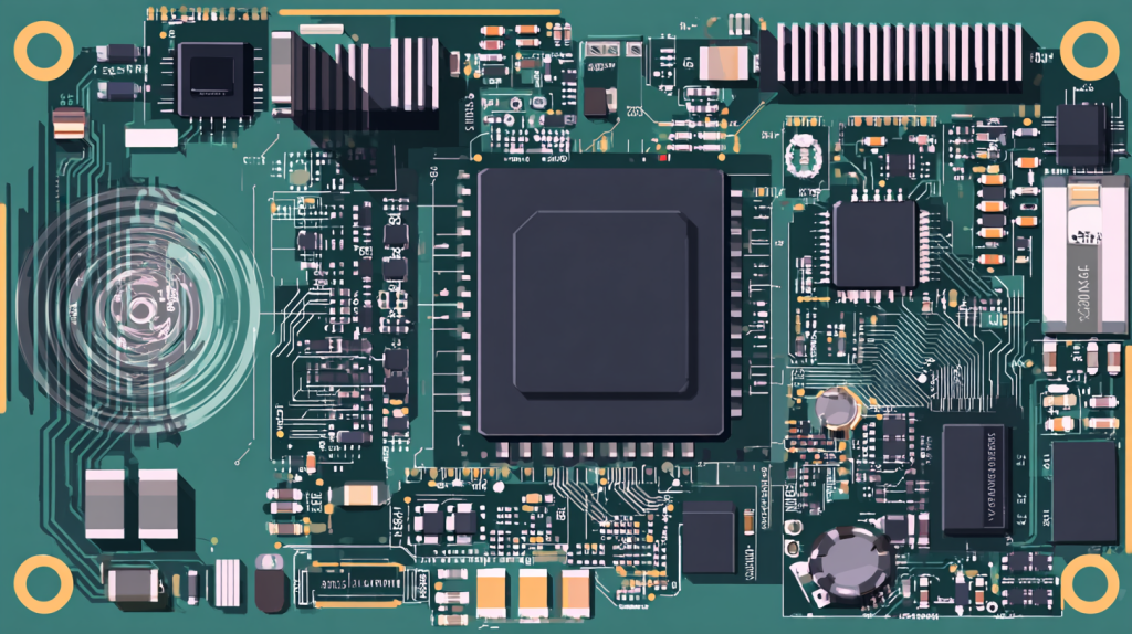
The analogy that “ICs are just smaller versions of multilayer PCBs” is not entirely without merit. As processes become more differentiated between PCB manufacturers and assemblers, PCB design may begin to embrace some of the same philosophies used by the IC design industry to deal with escalating complexity. DFM manufacturability analysis is especially important in complex PCB design and manufacturing processes.
1. Purpose-oriented design concept
The key to a DFM free design is to match the design rules and constraints to the capabilities of the PCB manufacturing and assembly supplier. Once the design rules and constraints are established, they become the review conditions that need to be followed at all times to ensure that the design is manufacturable. Problems that arise during design are easiest to identify and correct during the design phase. Having DFM awareness at the design stage can pay huge dividends. Identifying manufacturing issues during initial design also reduces the amount of time spent redesigning due to deviations from the development plan. As a result, designers can begin designing exciting new products instead of getting stuck in an avoidable redesign quagmire.
In order to provide a global DFM assessment, traditional DFM needs to be augmented by a Design for Availability assessment of components. The designer can open the Bill of Materials (BOM) at any time throughout the design process to get immediate real-time information on component availability. If a major component is out of stock, the system automatically creates a component from a selection of sequentially ranked parts from other manufacturers in the BOM. This process makes component sourcing more flexible, allowing designers to focus on the design while providing early warning of component supply risks.
● Bringing a global view of DFM into design can also improve designers’ skills, such as how to avoid triggering a DFM experience
The warning is a proof of the operation. Institutionalizing a global view of DFM within the design team can be a great way to raise the bar for the entire design team. This approach not only achieves DFM flexibility, but it also achieves the best of both worlds by not placing a lot of extra burden on the designers. In addition, as designers become more aware of DFM, their value in the industry will increase.
2. Understanding the ultimate goal
By adopting the definition of “beginning with the end in mind”, it is clear that it is essential for the designer to have a clear understanding of the end goal of the design. In PCB manufacturing and assembly, this means having a thorough understanding of the capabilities of the chosen manufacturing and assembly supplier. Typically, the supplier will detail this capability in a document that lists it, which must be translated into a set of rules and constraints that are applied in the PCB design environment.
While some manufacturers present their production capabilities in the form of rules documents that can be used immediately in the PCB design environment, there is no consistency among the thousands of PCB manufacturers and assembly service providers around the world. At the same time, the complexity of PCB design, manufacturing, and assembly continues to escalate, and capacity is becoming increasingly tight.
● Today, PCB design and manufacturing is seen as a very risky endeavor due to the very high cost of non-repeatable engineering. The costs are so high that it is important to get it right the first time. To achieve this, the industry has adopted a range of design methods and tools, thanks in part to multi-vendor support for library and design data exchange. This relatively open data exchange even includes portability of “rule sets” used by competing physical verification systems. By necessity, the approach considers manufacturing early in the design cycle.
3. Go boldly
The trend toward increased PCB complexity, density, and edge speeds shows no sign of slowing down, and there is even PCB-related research into interconnections using hybrid copper and embedded polymer waveguides. Combine this with the wider use of stacked packages and other newer assemblies.
Combined with technology, PCB manufacturing will become even more artistic than it is today. Just as semiconductor manufacturers such as Intel, Samsung, and TSMC closely guard their manufacturing IP to differentiate themselves, this will continue to have an impact on the PCB manufacturing space. Manufacturers and assemblers will continue to differentiate themselves through their manufacturing capabilities and proprietary IP technologies. With a fully connected and data-supported global ecosystem of manufacturers and assemblers, designers will have immediate visibility into the production capabilities of a manufacturer or electronics manufacturing contract service provider once they have selected one. Depending on the capabilities of the target manufacturer, the design space will adjust to the inherent rules and constraints that need to be applied to their design. This concept is similar to the way changes are previewed in the Print dialog box when different printers are selected. When you select a printer that supports color printing, the preview screen changes along with the available graphic resolutions, page sizes, and other printer-specific features.
This data-based global ecosystem can integrate manufacturing awareness into the product development process early in the design process, raising awareness of manufacturing capabilities and reducing or avoiding late-stage communication by eliminating the need to readily communicate through online meetings or e-mail. Assuming that an assembler adds a more powerful mounting line, the designers involved immediately realize that they need to update their rules and constraints to take this into account.
● If the design is complete, imagine being able to submit your PCB design to PCB manufacturers and assemblers around the world with the click of a mouse, and then find the supplier best suited to produce the design. After submitting your file, you’ll receive a list of companies with requirements that can manufacture it while meeting factors such as lead times, cost targets, current capacity, and geographic location.
4. Conclusion on DFM in the electronics industry
First pass design, high yields, cost optimization, and reliable PCB fabrication and assembly are the desired goals; quickly identifying and correcting DFM issues during the design phase is key to avoiding the submission of non-manufacturable designs. Enhancing traditional DFM inspection with real-time component intelligence helps eliminate the component shortage surprises that characterize many assembly lines today.
This global DFM awareness applied to the design of PCBs lays the foundation for a design process that not only adapts to design challenges, but also avoids compromising profitability, product development schedules, and industry reputation. As product complexity increases over time, global DFM awareness continues to be a strategically important capability that contributes to the certainty of electronic product realization.