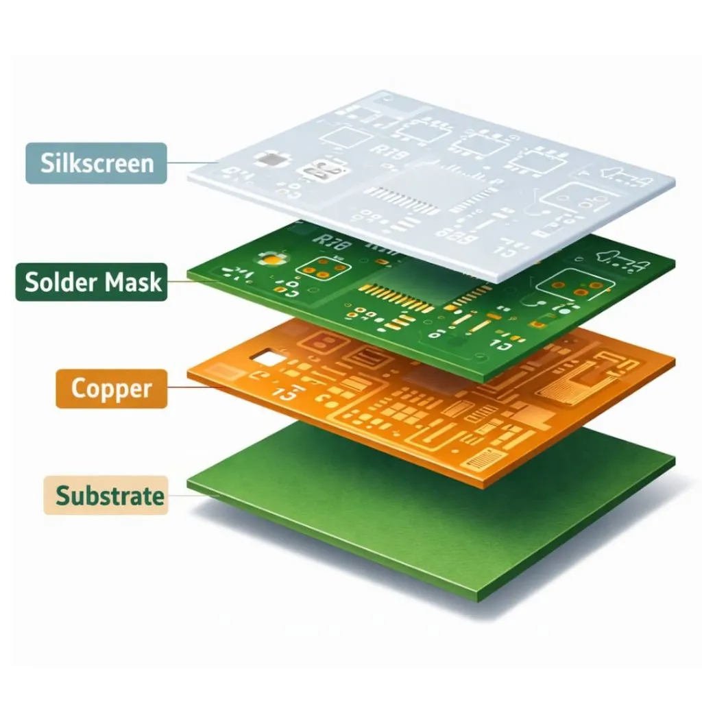
Gerber layers are individual vector graphic files. These files tell how your Printed Circuit Board will look. Gerber files tell physical aspects like copper traces, solder masks, and silkscreen. PCB manufacturers use these files to control every production step. You view these layers stacked from top to bottom, with the bottom layers mirrored for accurate fabrication.
Individual Files for Each Layer
Every real part of your PCB needs its own Gerber file. Like, you must have separate files for the top copper, the bottom copper, the paint for solder masks, the white silkscreen words, and the paste layers. If your PCB is a multilayer, you also need files for the inner copper layers! Every single layer is a separate file. This helps the factory to work on each part alone.
Viewing Gerber Layers
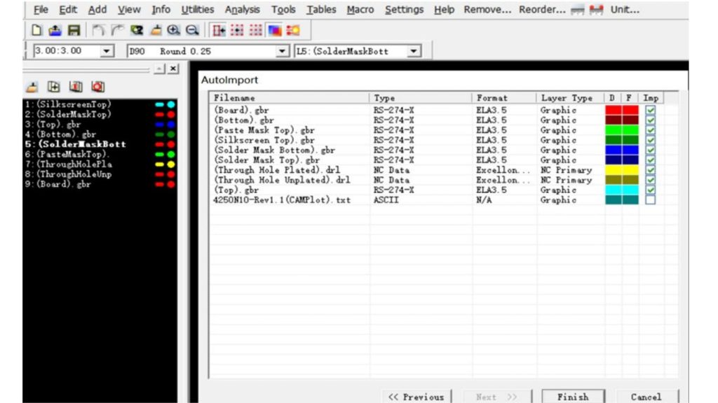
When you look at these files using a special online viewer, the software shows them all stacked up from top to bottom. This is like looking through a board made of clear glass! This view helps you check if the pads, vias, and traces are aligned correctly across all the layers. This is very important before you send the files to the factory for making.
Positive vs. Negative Layer Images
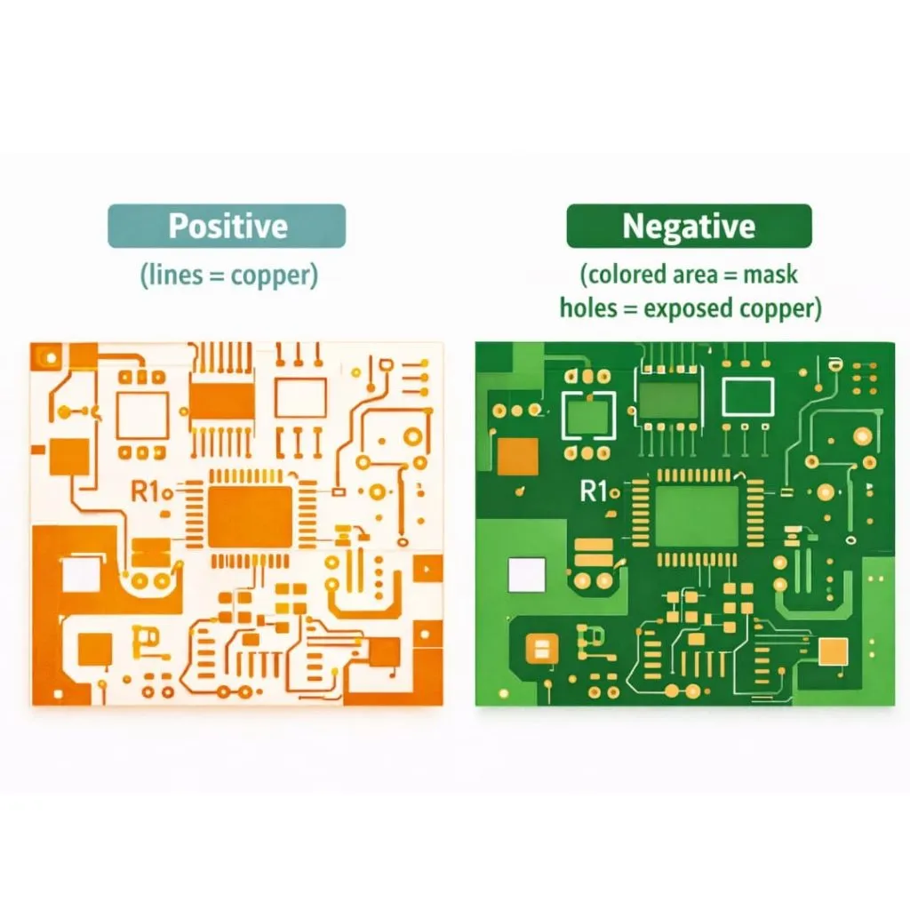
Gerber layers use either positive or negative imaging. Positive layers show copper presence as filled areas—common for copper layers where traces and pads appear solid. Negative layers work oppositely—filled areas indicate absence. Solder mask layer Gerber files use negative imaging, meaning filled regions represent openings where copper remains exposed.
Layer Naming Conventions and File Extensions
Standard Gerber file extensions follow predictable patterns. The top copper generally uses .GTL, bottom copper uses .GBL, and solder masks use .GTS and .GBS. Different software tools employ various naming conventions—Kicad Gerber layers use one scheme while gerber layers from altium follow another. Understanding these conventions prevents confusion when organising your fabrication package.
Copper Layers
Top Copper Layer
The top copper gerber layer contains all conductive features on your board’s upper surface. This includes signal traces, component pads, copper pours, and the top portions of vias. When you export gerber layers, the GTL file defines where copper remains after etching.
Bottom Copper Layer
Your bottom copper gerber layer mirrors the top layer’s function but for the underside of the board. This layer appears horizontally flipped when viewed from the top perspective. All bottom-side traces, pads, and copper fills reside in this layer.
Inner Signal Layers
Multilayer boards include inner layer gerber files between the top and bottom copper. These layers carry additional signals or provide dedicated routing space. You designate them as G1, G2, G3, and so on, based on their position in the stack. Each inner signal layer requires its own gerber file for fabrication.
Power and Ground Planes
Power and ground planes often use negative imaging. In these inner layer gerber files, filled areas represent copper removal rather than copper presence. This negative format efficiently describes large copper pours with clearances for vias and traces.
What Copper Layers Contain
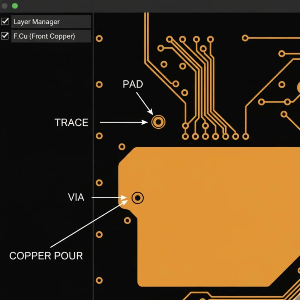
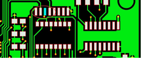
All copper layers describe four main feature types. Traces are the narrow lines connecting components. Pads provide mounting points for component leads and solder joints. Vias create electrical connections between layers. Copper pours fill larger areas for power distribution, ground planes, or thermal management.
Solder Mask Layers
Top Solder Mask Layer
The top solder mask layer gerber tells about the protective coating placement on your board’s upper surface. The purpose of this layer to stop solder bridges during assembly and protect copper traces from oxidation and physical damage.
Bottom Solder Mask Layer
Your bottom solder mask operates identically to the top layer but protects the underside. Both solder mask layers follow the same negative imaging convention.
Understanding Negative Image Concept
Solder mask layers confuse many designers because they use negative imaging. Filled areas in your gerber solder mask files indicate openings—places where solder mask will not be applied. These openings expose copper for component attachment and test points.
Solder Mask Openings Explained
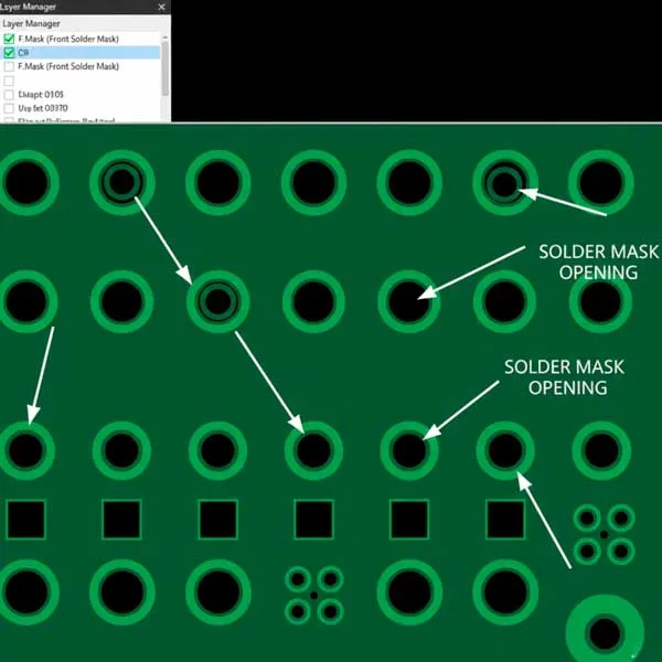
Solder mask openings appear wherever your board requires exposed copper. Component pads need openings for soldering. Test points require openings for probe access. Edge connectors need exposed copper for mating. Your design software automatically generates these openings based on pad and via locations.
Solder Mask Colors and Finishes
While gerber files define opening locations, manufacturers determine color and finish separately. Green remains the most common solder mask color, though manufacturers offer red, blue, black, white, and other options. The gerber file structure remains identical regardless of color choice.
Silkscreen Layers
Top Silkscreen Layer
The top silkscreen gerber layer contains printed markings visible on your finished board. This layer typically appears white or yellow on green boards but can vary with solder mask color choices.
Bottom Silkscreen Layer
Bottom silkscreen serves the same purpose as top silkscreen but appears on the underside. Many single-sided designs omit this layer entirely as it provides no functional value.
Silkscreen Content
Your silkscreen Gerber layer is very important for assembly technicians.
This layer has many things, like:
- The names of the parts like R1, C2, and U3
- The polarity markings for diodes and capacitors.
- The pin 1 indicator for the main chips.
- The company’s own logo.
- And instructions on how to put the board together.
Why Bottom Silkscreen Appears Mirrored
When viewing gerber layers from the top-down perspective, bottom silkscreen appears horizontally flipped. This mirroring ensures text reads correctly when you physically flip the board over.
When Silkscreen Layers Are Optional
You can manufacture PCBs without silkscreen layers. Simple designs, space-constrained boards, or products where markings compromise aesthetics may exclude silkscreen entirely. Manufacturers accept designs with missing silkscreen without issue.
Solder Paste Layers
Top Paste Layer
The top paste mask gerber defines stencil openings for automated solder paste application. This layer appears only in designs using surface mount technology (SMT) assembly.
Bottom Paste Layer
Your bottom paste layer functions identically to the top paste layer but defines stencil openings for bottom-side SMT components.
Purpose in Stencil Manufacturing
Manufacturers use paste mask gerber files to make metal and plastic stencils. In PCB assembly, PCB manufacturers align the stencil to your board. They squeegee solder paste through the openings onto pads.
Size Differences Between Paste and Solder Mask Openings
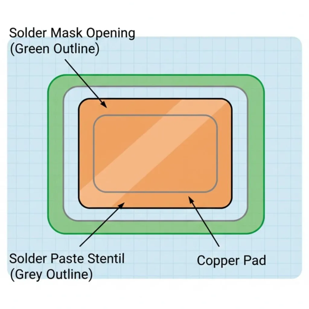
Paste layer openings typically measure slightly smaller than corresponding solder mask openings. This reduction controls solder paste volume, preventing excessive paste that could cause bridging. Some designs partition large pads into multiple smaller paste openings to further reduce paste volume.
SMT Assembly Applications
Only boards requiring automated assembly need paste layers. Through-hole only designs or hand-assembled prototypes can omit these layers. When you create gerber layers for SMT production, always include both paste layers if you have components on both sides.
Drill and Route Layers
Plated Through-Hole Drill Files
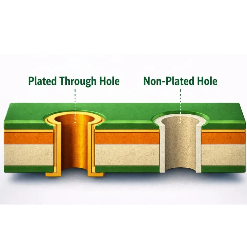
PTH drill files specify hole locations and sizes for plated holes. These holes receive copper plating during fabrication, creating electrical connections between layers. Component leads, vias, and test points use plated holes.
Non-Plated Through-Hole Drill Files
NPTH drill files define holes that remain unplated. Mounting holes, tooling holes, and mechanical features typically use non-plated holes to prevent unwanted electrical connections.
Via Drill Layers
Via holes appear in your PTH drill file but serve a specific purpose—layer interconnection rather than component mounting. Your gerber files define via pad sizes on copper layers while drill layers specify the hole diameter.
Blind and Buried Via Drill Data
Advanced multilayer designs may include blind vias or buried vias. These require special drill data specifying which layers each via connects, increasing manufacturing complexity and cost.
NC Drill Files vs. Gerber Files

Drill information traditionally uses Excellon format rather than gerber format. These .drl or .txt files use different syntax but serve the same purpose—telling drilling machines where to create holes and what size bit to use.
Excellon Format Explained
Excellon format lists drill coordinates and tool assignments in ASCII text. Each tool number corresponds to a specific drill bit diameter. The file format dates to older NC drilling machines but remains the industry standard.
Mechanical and Documentation Layers
Board Outline Layer
Your board outline layer defines the physical dimensions and shape of your PCB. Without this layer, manufacturers cannot determine where to route individual boards from production panels. This gerber file typically carries a .GKO or .GM1 extension.
Mechanical Layers for Slots and Cutouts
Mechanical layers describe non-electrical features like mounting slots, large cutouts for displays or connectors, and complex board shapes. You include these in your fabrication package alongside standard gerber layers.
Keep-Out Layer
Keep-out layers define restricted areas where components or routing cannot exist. While primarily a design rule, manufacturers may request this layer to understand assembly constraints or panel layout requirements.
Documentation Layers
Documentation layers provide human-readable information not directly used in fabrication. These may include dimension callouts, notes, or assembly instructions that complement your silkscreen information.
Drill Drawing Layers
Drill drawings show hole locations, sizes, and types in a visual format engineers can easily interpret. This layer supplements the machine-readable drill files, helping manufacturers verify hole placements before production.
Fabrication Notes and Instructions
You can include special fabrication instructions as text or drawing layers. These notes specify materials, finishes, testing requirements, or other manufacturing details not captured in standard gerber layers.
Specialized Gerber Layers
Assembly Layers
Assembly layers show component outlines, reference designators, and placement information. While similar to silkscreen, assembly layers serve manufacturing rather than final board marking. You typically export these separately from standard gerber layers.
V-Cut/Scoring Layers
V-cut layers define where manufacturers should score your board for easy separation from panels. These angled cuts allow breaking boards along predetermined lines without routing.
Gold Finger Layers
Edge connector designs require gold finger layers specifying which pads receive hard gold plating. This specialized finish provides superior wear resistance for repeatedly mated connectors.
Edge Plating Layers
Edge plating layers identify board edges requiring copper plating. This technique creates conductive surfaces along board perimeters for shielding or electrical continuity.
Test Point Layers
Test point layers identify specific pads or vias designated for automated testing. This information helps manufacturers program test fixtures and flying probe machines.
Layer Count and PCB Complexity
Single Layer PCB Gerber Files
Single layer designs do not need much of gerber files. For example, there is one copper layer, one solder mask, optional silkscreen, board outline, and drill file. Subsequently, the simple boards cost less and you can produce them faster.
Double-Layer PCB Gerber Files
Double-layer boards add bottom copper, bottom solder mask, and optional bottom silkscreen to the file set. This configuration suits most hobbyist and low-complexity commercial designs.
Multi-Layer PCB Gerber Files
Now, we talk about what happens when your PCB has many layers!
When you have more layers on a PCB, your Gerber package also increases. A six layer board has files for top copper, four inner layers, and bottom copper, plus the files for the solder mask, silkscreen, and paste layers. Some very difficult designs also have 20 or more layers! Each one needs its own Gerber file.
How Layer Count Affects Design Capability
These extra layers give you more space for routing. This means you can put the parts closer together and make more complex circuits. The inner layers can be used as special planes for power and ground. This makes the signal quality better and it helps to stop electrical noise.
Performance Differences Based on Layer Count
Higher layer counts enable controlled impedance routing, better power distribution, and improved signal integrity. However, they increase cost, manufacturing time, and design complexity. You should select layer count based on electrical requirements rather than arbitrary preferences.
Common Gerber Layer File Extensions
| Layer Type | Extension | Meaning |
| Top Copper | .GTL | Gerber Top Layer |
| Bottom Copper | .GBL | Gerber Bottom Layer |
| Top Solder Mask | .GTS | Gerber Top Soldermask |
| Bottom Solder Mask | .GBS | Gerber Bottom Soldermask |
| Top Silkscreen | .GTO | Gerber Top Overlay |
| Bottom Silkscreen | .GBO | Gerber Bottom Overlay |
| Top Solder Paste | .GTP | Gerber Top Paste |
| Bottom Solder Paste | .GBP | Gerber Bottom Paste |
| Board Outline | .GKO | Gerber Keep-Out |
| Drill File | .DRL / .TXT | Drill Data |
Standard Extensions
Industry standard extensions tell the layer identity. For example, GTL tells about top copper, .GBL bottom copper, .GTS top solder mask, .GBS bottom solder mask, .GTO top silkscreen, and .GBO bottom silkscreen. Inner layers use .G1, .G2, .G3, and so on.
KiCad Layer Extensions
When you export gerber layers from KiCad, the software uses descriptive extensions. These are .F.Cu for front copper, .B.Cu for back copper, .F.Mask for front solder mask, and .B.Mask for back solder mask. This naming convention improves readability but differs from traditional standards.
KiCad uses a very logical naming system that includes the layer name directly in the extension.
- Copper: .F.Cu, .B.Cu
- Solder Mask: .F.Mask, .B.Mask
- Silkscreen: .F.SilkS, .B.SilkS
- Edge Cuts: .Edge.Cuts
Altium Designer Layer Extensions
Altium usually follows the Protel standard but uses .GM1, .GM2, etc., for Mechanical Layers. Usually, .GM1 is used for the board outline instead of .GKO.
Eagle Layer Extensions
Eagle gerber layers export uses .cmp for top copper, .sol for bottom copper, .plc for silkscreen, and .stc for solder mask. These extensions originate from older PCB terminology.
- Top Copper: .cmp
- Bottom Copper: .sol
- Top Silkscreen: .plc
- Top Solder Mask: .stc
Generic .GBR Extension
Some software exports all layers with generic .gbr extensions. They rely on file names rather than extensions for layer identification. This approach requires careful file organization and clear naming to avoid confusion.
Because of the confusion caused by all these different extensions, the industry created Gerber X2.
- The Extension: Every single file ends in .GBR.
- How it works: The information about what the layer “is” is actually written as metadata inside the file.
- Benefit: There is no need to take tension about extensions at all; the manufacturer’s software read the internal tags to identify the layers automatically.
Analyzing Gerber Layers
Using Gerber Viewer Software
Free gerber viewer layers tools let you inspect your files before fabrication. These applications display individual layers or combined views, helping you verify design intent. Popular options include online gerber file viewers and downloadable desktop applications.
Layer-by-Layer Inspection Process
You should examine each layer independently. For example, you will verify trace widths, clearances, and feature placement. Check that copper layers contain expected routing, solder masks have appropriate openings, and silkscreen text remains legible and properly positioned.
Comparing Layers for Alignment
Gerber layers alignment is critical for functional boards. Use your viewer to overlay multiple layers, checking that pads align across copper and solder mask layers, vias connect intended layers, and drill holes center properly on pads.
Identifying Layer Functions
Sometimes you receive gerber files with unclear naming. A gerber layers editor helps identify layer functions by examining content—copper layers contain traces and pads, solder masks show negative openings, silkscreen displays text and graphics.
2D vs. 3D Visualization
Advanced gerber viewers offer 3D visualization, showing your board as it will appear when manufactured. This perspective helps identify clearance issues, component conflicts, and aesthetic concerns invisible in 2D views.
Common Layer-Related Issues
Missing Required Layers
The most common problem is missing gerber layers in your fabrication package. Manufacturers cannot proceed without board outline files. Missing solder mask or drill files creates ambiguity about your intentions. Before submission, verify your package includes all essential layers.
Incorrect Layer Polarity
Layer polarity errors occur when positive layers export as negative or vice versa. This mistake typically affects solder mask layers, where incorrect polarity creates boards with inverted mask coverage—coating where it should open and opening where it should coat.
Misaligned Layers
Gerber layers not matching different origin points cause misalignment. This happens when some layers reference one coordinate system while others use different origins. The result is copper pads not centering under solder mask openings or drill holes missing their intended pads.
Improper Layer Naming
Ambiguous file names cause confusion and potential fabrication errors. When manufacturers cannot determine which file represents which layer, production halts pending clarification. Use clear, standard naming conventions to prevent these delays.
Solder Mask vs. Paste Layer Confusion
Designers sometimes confuse solder mask and paste layers, submitting one when manufacturers need the other. Solder mask defines permanent board coating while paste layers create temporary stencils for assembly. These serve completely different purposes.
Best Practices for Gerber Layer Management
Verifying All Necessary Layers Are Included
Before sending files, create a checklist of required layers. Minimum requirements include top copper, board outline, and drill file. Two-layer boards add bottom copper and typically both solder masks. SMT designs require paste layers. Multilayer boards need all inner copper layers.
Using Consistent Naming Conventions
Adopt a clear naming scheme and apply it consistently across projects. Include layer function and, if helpful, project name in each file name. This practice prevents confusion when working with multiple designs simultaneously.
Layer Documentation Guidelines
Create a simple text file listing all included gerber layers with descriptions. This readme file helps manufacturers verify they received complete packages and understand any non-standard naming you employed.
Communicating Layer Requirements to Manufacturers
Contact your manufacturer before finalizing gerber layers for pcb fab. Different facilities have varying preferences for file formats, naming, and package organization. Aligning with their requirements prevents manufacturing delays.
Quality Checks Before Submission
Load your complete gerber package into a viewer and perform thorough checks. Verify board dimensions match your design intent. Confirm all layers align properly. Check that solder mask openings expose intended pads. Ensure silkscreen text does not overlap pads or extend beyond board edges. Review drill holes for correct sizes and placements. These checks catch most gerber layer problems before they impact production.
Conclusion
Each gerber layer is for a specific purpose for PCB manufacturing and assembly. Top and bottom copper gerber files define conductive pathways. Solder mask layers protect copper while exposing important connection points. Silkscreen layers guide assembly and maintenance. Paste layers enable automated solder application. Drill files specify interconnections between layers. Together, these gerber format layers provide manufacturers with complete instructions for building your boards.