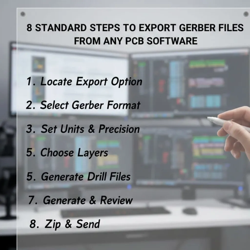
There are 8 standard steps to export Gerber files from any PCB software. These are:
- Locate Export Option
- Select Gerber Format
- Set Units & Precision
- Choose Layers
- Generate Drill Files
- Specify Output
- Generate & Review
- Zip & Send
So this is basically a beginner guide that will share steps to export gerber files from any PCB software such as Kicad, Altium, Eagle, and Easy Eda.
What Are Gerber Files?
Gerber files are industry-standard files that contain layer-by-layer information about your PCB design. Each file describes a specific layer of your board. Your design software creates these files when you export your finished design. The files use ASCII text format that fabrication machines can read and process.
Why Gerber Files Are Important for PCB Manufacturing
Manufacturers rely on Gerber files to control every step of PCB fabrication. The files tell machines where to etch copper traces, drill holes, and apply solder mask. Without proper Gerber files, your manufacturer cannot build your board.
How often do you check your files before sending them to production? Most designers skip this step and face delays. You should verify every file to avoid costly mistakes.
Common Gerber File Formats
Three main Gerber formats are there:
- RS-274-D is obsolete and manufacturers no longer accept it.
- RS-274-X solved the problems of the old format.
- Gerber X2 is the latest standard released in 2014.
Understanding Gerber File parts
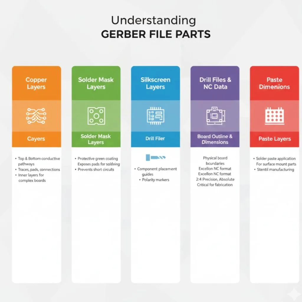
Your complete PCB design requires multiple Gerber files working together. Each file shows one physical or functional layer of your board.
Copper Layers
Copper layers tell the conductive pathways on your PCB. The top copper layer contains traces, pads, and connection points on the board’s upper surface. You will find part connections and signal routing in this layer.
The bottom copper layer works the same way but on the opposite side. Both layers show where copper should remain after etching. Most simple designs use just two copper layers. But complex boards can have many internal layers.
Solder Mask Layers
Solder mask layers control where the green coating appears on your board. This protective layer covers copper traces but leaves pads exposed for soldering.
You need separate files for top and bottom solder masks. The solder mask stops accidental short circuits during assembly.
Silkscreen Layers
Silkscreen layers contain text, labels, and part outlines. You use these markings to show part placement, polarity markers, and reference designators. White ink typically prints these details on the board surface.
Your silkscreen helps during assembly and troubleshooting. Clear labels prevent parts from being installed backwards. You should avoid placing silkscreen over pads or areas that need soldering.
Drill Files and NC Data
Drill files specify hole locations and sizes throughout your board. These files are technically not Gerber format but use Excellon NC format. Manufacturers often call them NC drill files or just drill files.
Your drill file must include proper header information. The format should specify 2.4 precision, absolute coordinates, and trailing zeros. Without correct formatting, manufacturers struggle to import your drill data. This often results in trial and error attempts that delay production.
Board Outline and Dimensions
The board outline tells your PCB’s physical boundaries. This layer shows where machines should cut or route the individual boards from the manufacturing panel. Your outline also includes any cutouts or special shapes.
Some design software does not generate board outlines by default. You must specifically enable this option during export. The outline can appear as a separate Gerber file or within your drill file. Missing board outlines are one of the most common problems that halt production.
Paste Layers
Paste layers tell where solder paste should be applied for surface mount parts. Stencil manufacturers use these files to create solder paste stencils. You need separate paste layers for top and bottom surfaces.
Pre-Export Checklist
You must verify your design before generating Gerber files. Errors found after manufacturing cost significant time and money.
Completing Your PCB Design
First, you need to finish all design work completely. This means finalizing part placement, completing all routing, and adding necessary labels. You should review your schematic one final time to ensure it matches your layout.
Check that all required circuits are present and functional. Verify power and ground connections are solid. Make sure you have placed mounting holes and any mechanical features. Your design must be 100% complete before you proceed to export.
Running Design Rule Checks)
Then, you should run a comprehensive Design Rule Check. This automated process finds electrical and mechanical errors in your design. The DRC verifies trace widths, clearances, and spacing rules.
You will need to fix every error the DRC reports. Some warnings might be acceptable, but you must understand why they appear. Never ignore DRC errors because they often indicate serious problems. Most software will not allow you to export if important errors exist.
Verifying part Placement
Next, inspect your part placement carefully. Make sure parts do not overlap and have adequate spacing for assembly. Check that polarized parts face the correct direction. Verify that mounting holes align with your enclosure.
You should confirm that all footprints match your actual parts. Wrong footprints are a common mistake that ruins boards. Take time to measure important parts against their footprints.
Checking for Flying Wires and Errors
Finally, make sure no unrouted connections remain. Flying wires indicate incomplete routing that will cause board failure. Your software should highlight these clearly in the design view.
Look for traces that end in empty space or pads without connections. Check that all required nets are properly routed. A single missed connection makes your entire board non-functional. This simple check prevents complete board failures.
Exporting Gerber Files from KiCad
KiCad offers a straightforward process for generating Gerber files. This free software produces reliable output files that manufacturers accept.
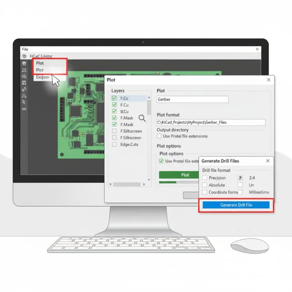
Step 1: Opening the Plot Dialog
First, you need to open your completed PCB file in KiCad’s PCB Editor. Look for the File menu at the top of the screen. Select Plot from the dropdown menu to launch the Gerber generation tool.
The Plot dialog window will open with multiple options. This interface controls all Gerber export settings. You should see a list of layers on the left side and configuration options on the right.
Step 2: Selecting Layers and Output Settings
Then, you should select which layers to export. Tick the checkboxes next to each required layer. For a standard two layer board, you need:
- F.C
- B. Cu
- F.Mask
- B.Mask
- F.Silkscreen
- B.Silkscreen
- and Edge.Cuts.
Set the output format to Gerber from the dropdown menu. Your next step is to choose an output directory where files will be saved. You should create a dedicated folder for your Gerber files. Then, Set the Plot format options to use Protel extensions if your manufacturer prefers them.
Step 3: Generating Gerber Files
After that, click the Plot button at the bottom of the dialog. KiCad will process each selected layer and create individual Gerber files. After that, the software will show a progress message as it generates files.
You can verify the files were created by checking your output directory. Each layer should have its own file with an appropriate extension. The number of files will match the number of layers you selected.
Step 4: Exporting Drill Files
Finally, make sure to generate your drill files separately. Click the Generate Drill Files button in the Plot dialog. A new window will open with drill file options.
Use the default Excellon format with 2:4 precision. Select Absolute for coordinate format and Millimeters or Inches based on your manufacturer’s requirements. Click Generate Drill File to create the NC drill data. Your drill file will appear in the same output directory as your Gerber files.
Exporting Gerber Files from Altium Designer
Altium Designer provides powerful Gerber export capabilities. The software offers precise control over every export parameter.
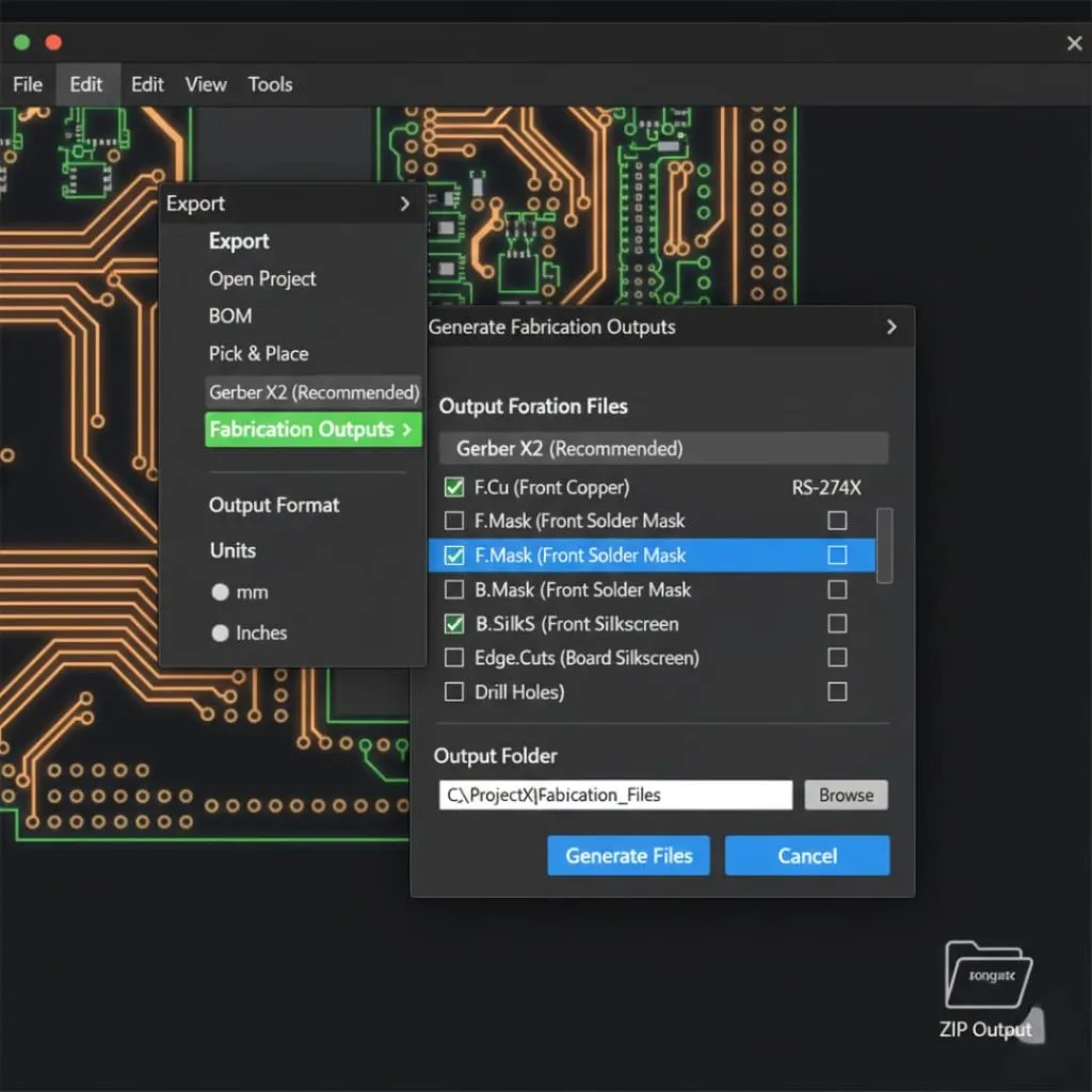
Step 1: Accessing Fabrication Outputs
First, you need to open your PCB project in Altium Designer. Navigate to the File menu and find Fabrication Outputs. Hover over this option to see a submenu appear.
Select Gerber Files from the submenu. This action opens the Gerber Setup dialog with comprehensive export options. You will configure all settings from this central interface.
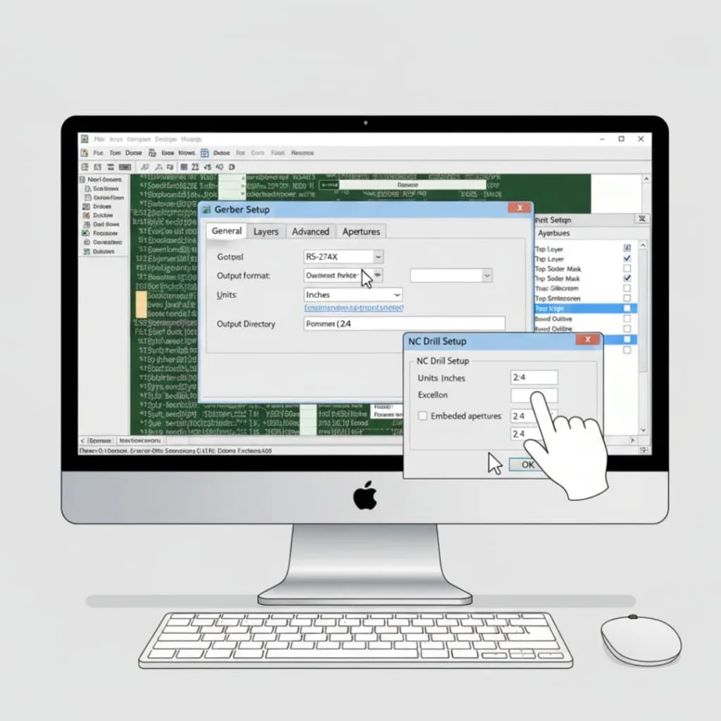
Step 2: Configuring General Settings
Then, you should configure the general settings tab. Select the output format as RS-274X for maximum compatibility. Choose your preferred units based on manufacturer specifications.
Set the format to 2:4 for inches or 3:4 for millimeters. These precision settings ensure accurate coordinate showation. You should also specify an output directory for your files.
Step 3: Layer Configuration
After that, move to the Layers tab. This section displays all available board layers. You need to select which layers to include in your Gerber output.
Check the boxes for all necessary layers including signal layers, mask layers, silkscreen, and mechanical layers. Altium will create one Gerber file for each selected layer. Make sure you include the board outline layer for proper dimensioning.
Step 4: Aperture Settings
Next, configure the aperture settings carefully. Apertures tell the shapes and sizes of pads and traces in your Gerber files. Use embedded apertures rather than separate aperture files.
Set the aperture format to match your precision settings. This ensures consistency across all files. Most manufacturers prefer embedded apertures because they eliminate compatibility issues.
Step 5: Generating NC Drill Files
Finally, make sure to generate NC drill files separately. Return to the File menu and select Fabrication Outputs then NC Drill Files. Configure the drill file settings to match your Gerber precision.
Select the appropriate units and format. Use Excellon format for maximum compatibility. Click OK to generate your drill files. Altium will create separate files for plated and non-plated holes if your design includes both types.
Exporting Gerber Files from Eagle
Eagle uses a CAM processor for Gerber generation. This system provides flexibility but requires understanding the process.
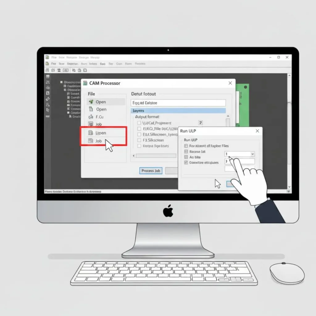
Step 1: Opening the CAM Processor
First, you need to open your finished board file in Eagle. Click on File in the menu bar, then hover over CAM Processor. This will display CAM-related options.
Select CAM Processor to open the main export interface. You will see a window with multiple tabs and processing options. Eagle uses job files to control the export process.
Step 2: Loading the Gerber CAM Job
Then, you should load a pre-configured CAM job file. Click on File within the CAM Processor window and select Open” then Job. Navigate to Eagle’s CAM folder to find standard Gerber job files.
Look for files named gerb274x.cam or similar names indicating Gerber export. Load this job file to automatically configure all layers and settings. The job file includes instructions for generating all necessary Gerber files.
Step 3: Processing Job Files
After that, review the loaded job settings. Each tab in the CAM Processor shows one output file. You should see tabs for top copper, bottom copper, masks, silkscreen, and outline.
Verify that the output directory is correct. You can modify the save location if needed. When everything looks correct, click the Process Job button. Eagle will generate all Gerber files according to the job specifications.
Step 4: Generating Drill Files
Finally, make sure to export drill data separately. The standard Gerber CAM job might include drill file generation, but you should verify this. If not included, you need to run a separate drill file export.
Go to File menu and look for Run ULP. Find and execute the drill export script. This creates your Excellon drill file with proper formatting. Check that your output folder contains both Gerber and drill files before sending to manufacturing.
Exporting Gerber Files from Other Popular PCB Software
Different software packages have unique export procedures. Understanding these variations helps you work with any tool.
EasyEDA/EasyEDA Pro Export Process
EasyEDA offers a simple export process suitable for beginners. Open your completed design and click on “Fabrication Output” in the top menu. Select “Generate Gerber” from the dropdown options.
The software will automatically create all necessary files. EasyEDA includes proper layer naming and formatting by default. You can download the generated files as a ZIP archive. This convenient format is ready to send directly to most manufacturers.
DipTrace Export Steps
DipTrace provides straightforward Gerber export functionality. Navigate to “File” menu and select “Export” then “Gerber.” A dialog window will appear with layer selection options.
Choose all required layers for export. Set your coordinate format to 2:4 for inches. You should use vector fonts rather than TrueType fonts to avoid compatibility issues. Some older DipTrace versions had problems exporting with TrueType fonts. Generate your Gerber files, then export drill files separately through the “File” menu.
OrCAD and Cadence PCB Editor
OrCAD and Cadence PCB Editor use artwork creation for Gerber generation. Access the “Manufacture” menu and select “Artwork.” This opens the artwork control interface.
tell your artwork parameters including layer selection and output format. Use Gerber RS-274X format for compatibility. Configure film control options to set precision and units. You will need to create artwork for each layer type separately. The process requires more manual setup compared to other software.
Proteus PCB Export
Proteus handles Gerber export through its output menu. Open your PCB layout and click “Output” in the menu bar. Select “Generate CAM/NC Data” to access export options.
Configure the CAM processor settings for Gerber format. Select individual layers and set output parameters. Proteus generates files with generic extensions that you might need to rename. Create your drill file through the same output menu using NC drill format.
Post-Export Verification
You must verify your Gerber files before sending them to manufacturing. This important step prevents expensive mistakes.
Using Gerber Viewer Software
First, you need to load your files into a Gerber viewer. Free viewers include GerbView, ViewMate, or online viewers. Open each Gerber file individually to inspect it.
Look at the displayed image carefully. You should see clear traces, pads, and board features. Zoom in to check fine details. Compare what you see against your original design. Each layer should match your expectations.
Checking Layer Alignment
Then, you should verify that all layers align correctly. Load multiple layers simultaneously in your viewer. The viewer will overlay them to show how they relate to each other.
Your copper layers should align with pad locations. Solder mask openings should center over pads. Silkscreen should not cover pads or interfere with parts. Misaligned layers indicate export problems that will cause board failures.
Verifying Drill Holes and Placement
After that, inspect your drill file thoroughly. Load it alongside your copper layers in the viewer. Drill holes should appear at every pad location that needs drilling.
Check hole sizes against your design specifications. Verify that plated and non-plated holes are correctly identified. Look for missing holes or holes in wrong locations. This often happens when drill files export with incorrect settings.
Inspecting Aperture Information
Next, examine the aperture information in your files. RS-274X Gerber files include embedded aperture definitions. You should see various aperture codes for different pad and trace sizes.
Verify that aperture sizes match your design requirements. Incorrect apertures result in pads that are too large or too small. Your viewer might show aperture information in a table or list format.
Measurement Tools and Quality Control
Finally, make sure to measure important dimensions. Most viewers include measurement tools. Use these to verify trace widths, clearances, and pad sizes.
Measure the overall board dimensions against your specifications. Check that mounting holes are correctly positioned. Verify any important spacing requirements. These measurements confirm your files are accurate before manufacturing.
Best Practices for Gerber File Generation
Following industry best practices produces reliable Gerber files. These guidelines help you avoid common problems.
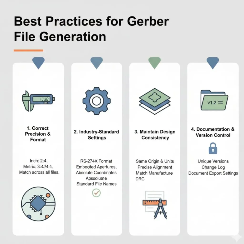
Setting Correct Precision and Format
First, you need to use appropriate precision settings. For inch-based designs, use 2:4 format. For metric designs, use 3:4 or 4:4 format.
Higher precision prevents rounding errors in coordinates. This matters most for fine-pitch parts and dense designs. Your manufacturer can handle the precision better than lower settings. Always match precision across all files to maintain consistency.
Using Industry-Standard Settings
Then, you should stick to proven settings that manufacturers expect. Use RS-274X format rather than obsolete formats. Select embedded apertures instead of separate aperture files.
Follow standard file extensions and naming conventions. Use absolute coordinates rather than relative coordinates. These standard settings eliminate compatibility issues. Your manufacturer’s processing will be faster and more reliable.
Maintaining Design Consistency
After that, verify consistency throughout your design. All layers should use the same coordinate system origin. Copper, mask, and silkscreen must align precisely.
Check that your design rules match manufacturer capabilities. Verify minimum trace widths and clearances are achievable. Consistency in design standards ensures manufacturable boards. This helps you avoid redesigns and production delays.
Documentation and Version Control
Finally, make sure to maintain good documentation and version control. Save each design revision with a unique version number. Keep notes about changes between versions.
Document your export settings for future reference. This helps when you need to regenerate files or make revisions. Good version control prevents confusion when you submit multiple iterations. Your manufacturer can track which version to produce.
Conclusion
Exporting Gerber files correctly ensures successful PCB manufacturing. You now understand the complete process from design completion to file delivery.
You learned to verify your design before export using DRC and visual inspection. Then you export Gerber files using your specific software’s procedure. After that, you verify the files using viewer software to catch errors. Finally, you package everything properly with clear documentation.