The solder mask layer on a PCB refers to the part of the board covered with green solder resist ink. Areas with solder mask openings are left without ink, exposing the copper for surface treatment and soldering components. Areas without openings are covered with solder mask ink to prevent oxidation and leakage.
Three Reasons for Solder Mask Openings:
1. Through-Hole Pad Openings:
Through-hole pads require solder mask openings. Without these openings, the soldering points will be covered by ink, making it impossible to solder component leads.
2. SMD Pad Openings:
Solder mask openings are required for SMD pads to allow soldering. If the soldering area lacks openings, the pads will be covered by ink, effectively rendering them unusable.
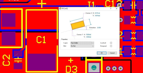
3. Large Copper Area Openings:
To increase current capacity without widening traces, certain areas are tin-plated. Tin-plating requires solder mask openings in these areas.
Why Solder Mask Openings Are Larger Than Pads
Solder mask openings are generally larger than the pads to account for manufacturing tolerances. If the solder mask opening is the same size as the pad, production variances could lead to solder mask ink covering part of the pad. To prevent this, solder mask openings are typically enlarged by 4-6 mils beyond the pad dimensions, considering standard PCB manufacturing tolerances.

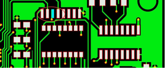
Causes of Solder Mask Omission
1. Gerber File Errors:
During the layout process, a designer may accidentally omit solder mask openings in the Gerber file due to incorrect settings or mistakes. If the solder mask layer is not properly configured to include pad openings during Gerber output, the resulting file will lack the necessary openings.
2. Incorrect Package Design:
Errors in the PCB package design can lead to missing solder mask openings. The solution is to configure the pad properties correctly. In the pad stack manager, add the Soldermask Top (or Bottom) and adjust the Soldermask shape to achieve the desired opening.
3. Software Version Incompatibility:
Differences between EDA software versions can cause solder mask omissions. For instance, using a high-version AD software where pads are defined using the Track function might lead to issues when the Gerber file is opened in a lower version. In older versions, tracks do not generate solder mask openings, whereas high-version AD software assigns special attributes to tracks.
4. Incorrect Via Attributes:
In AD software, adding pads using VIA instead of PAD can lead to solder mask issues. Vias typically have a default solder mask covering unless manually configured otherwise. If vias requiring solder mask openings are added incorrectly, they may be covered during fabrication.

5. File Modifications:
During iterative updates, redesigns, or board file copying, solder mask openings may accidentally be deleted due to user error, resulting in missing openings in the final design and preventing proper soldering.
By addressing these common causes and following proper design practices, solder mask omissions in PCB designs can be minimized, ensuring reliable soldering and functionality.