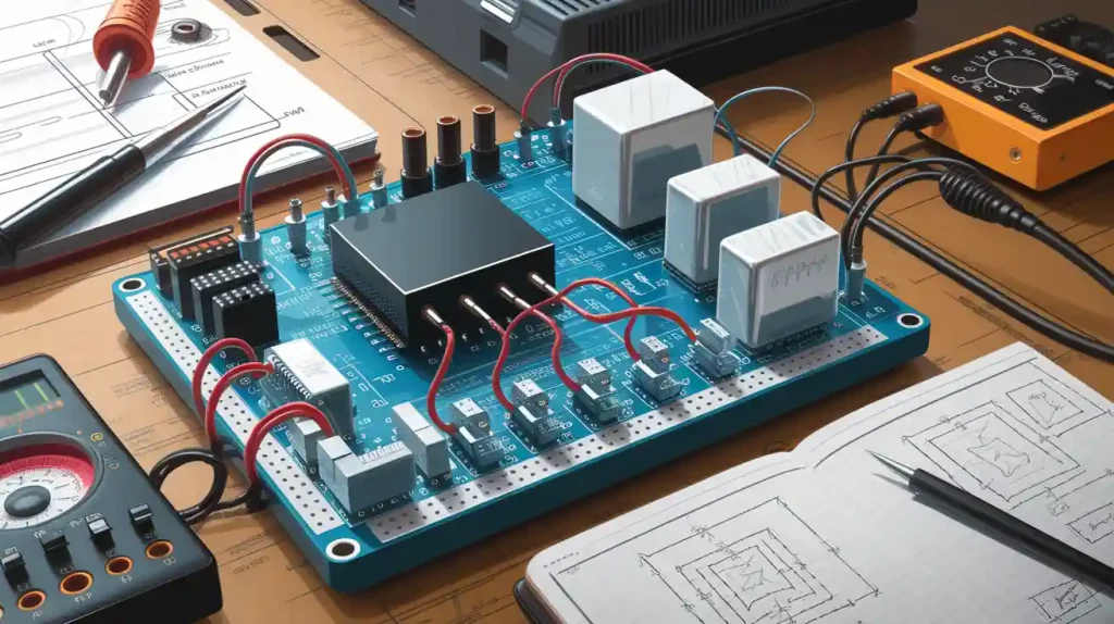
You may ask what makes hardware design different from PCB design. Hardware design is about planning the whole system and picking the best electronic parts. PCB design is about how these parts are put together on a board. Knowing this difference can help you be a better engineer or designer.
Hardware design and PCB design need different skills.
Each one deals with a different step in making an electronic device.
What is hardware design?
Hardware design means planning and making electronic devices. First, you figure out what the device should do. Next, you decide how the parts will work together. This helps your device work well and last a long time.
System Architecture
System architecture is a big part of hardware design. You make a plan that shows how all the parts connect. This lets you see how everything fits before you work on details. Here are the main steps in hardware design:
Make a list of what the device must do. You say how fast it should be and what rules it must follow.
Plan the electrical architecture. You choose how things like the processor and memory work together. You also decide how software and hardware will share jobs.
Build the design. You use special tools to draw the first pictures and layouts for your circuit board.
Each part changes how your device turns out:
Description | |
|---|---|
Processor and Memory | These decide how fast your device is and how much it can hold. |
Input/Output Interfaces | These help your device talk to people or other machines. |
Power Systems | These control energy, which matters for portable devices. |
Processing Speed | A good plan makes your device fast and easy to use. |
Battery Life | Smart power systems help your device last longer. |
Durability | Strong design keeps your device safe in hard places. |
Component Selection
Picking the right parts is very important in hardware design. You look for parts that fit your needs and work well together. Your choices change how well your device works and how easy it is to build and fix.
Criteria | Impact on Performance |
|---|---|
Compatibility | Makes sure all parts work together without problems. |
Quality Control | Lowers the chance of broken parts and helps reliability. |
Performance Requirements | Helps your device work safely and well. |
Availability | Keeps your project on time and on budget. |
Lifecycle Considerations | Makes your device easier to fix and keep working. |
Good hardware quality keeps your work going well.
Smart choices make building easier.
Good parts mean you fix fewer problems.
New parts keep your device safe and working right.
Tip: When you focus on hardware design, you help your circuit board and product work better.
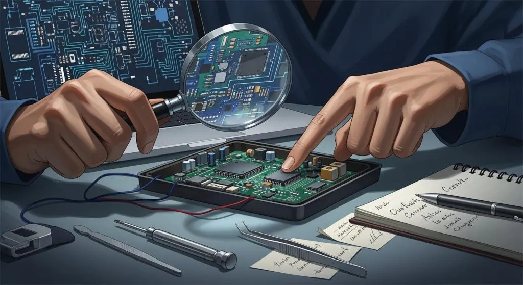
What is pcb design?
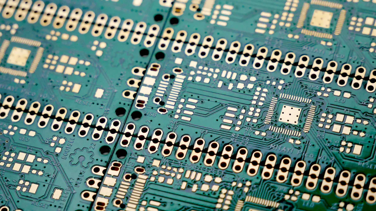
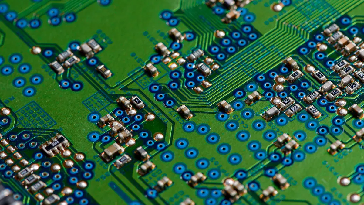
PCB design is a special job in electronics. It helps make the main part of many devices. In pcb design, you connect all the electronic parts. Printed circuit boards hold the parts and give them paths for electricity. They help your device stay small and work well.
Layout and Routing
You begin pcb design by making a layout. This means you pick where each part goes. Good placement helps your device work better. It also makes building easier. After placing parts, you draw traces. Traces are thin copper lines that link the parts. They let electricity move between them.
Here are the main steps you follow:
Put parts in good spots to save space.
Draw traces to connect all the parts.
Check if your design works and will last.
You must think about signal integrity. For example, keep weak signals away from noisy spots. Put bypass capacitors close to power pins. These choices help your device work well.
Section | Guidelines |
|---|---|
Trace Routing Readiness | Line up traces with parts and keep bypass caps close. |
Routing High-Speed Circuits | Keep traces short and put sensitive signals inside the board. |
Differential Pairs | Keep pairs together and do not split them. |
Length-Matched Nets | Make sure some traces are the same length. |
Avoid Noisy Areas | Keep weak traces away from power and analog spots. |
Minimize Via Usage | Use as few vias as you can to keep signals strong. |
Tip: Careful layout and routing help your board pass tests and work well.
CAD Tools
You use CAD tools to design printed circuit boards. These programs let you draw your board and check your work. They help you get files ready for making the board. Modern CAD tools have libraries, 3D views, and error checks. You can find problems before you build.
Some popular CAD tools are:
OrCAD for fast designs and checking signals.
Allegro PCB Designer for big, complex boards.
DipTrace for easy drag-and-drop design.
EasyEDA for working online and saving in the cloud.
Fusion 360 for mixing electronics and mechanical parts.
Many CAD tools now have built-in libraries and 3D views. You can work with your team online using the cloud. Some tools use AI to help you design faster and make fewer mistakes.
CAD Tool | Key Features | Best For |
|---|---|---|
OrCAD | Checks signals and has a big part library | Fast, professional designs |
Allegro PCB Designer | Fast routing and works with MCAD | Big, high-performance boards |
DipTrace | Drag-and-drop, auto-routing, 3D modeling | Beginners and cheap projects |
EasyEDA | Cloud storage, works in browser, auto-routing | Teamwork and easy access |
Fusion 360 | Mixes PCB with CAD/CAM/CAE | Electronics and mechanical projects |
Note: The right CAD tool makes pcb design faster and more correct.
Key Differences
Focus and Scope
It is important to know that hardware design and pcb design do different jobs. Hardware design is about planning the whole system. You pick the best parts and make sure they work together. Pcb design is about putting these parts on a board and connecting them with copper lines. Each job has its own goals and problems.
Here is a table that shows how their focus and scope are not the same:
Aspect | Hardware Design | PCB Design |
|---|---|---|
Scope of Work | Involves selecting and integrating components for devices | Focuses on arranging components and establishing connections |
Focus | Centers on practicality and efficiency | Prioritizes reliability and efficient use of space |
Complexity | Requires careful planning for component integration | Involves developing a complex layout to mitigate issues |
Tools and Software | Uses CAD for circuit design | Utilizes specialized software like Altium Designer |
When you do hardware design, you think about how each part helps your device. You want your device to be fast, safe, and easy to use. Pcb design is about fitting all the parts on a board and making sure it is strong. You use special software to draw the board and check for errors.
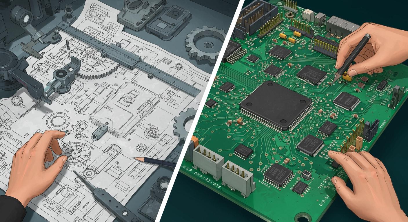
Process and Workflow
There is a clear order when you make electronic products. Hardware design comes first. You start by learning what your device should do. You talk to people and look at what is needed. You make a plan and pick the right parts. Only after hardware design is done do you start pcb design.
Here is a table that shows how the work moves from hardware design to pcb design:
Hardware Development Lifecycle Phases | PCB Design Involvement |
|---|---|
Requirements or ideation | Involves gathering requirements for PCB design |
Design | PCB design occurs in this phase |
Manufacturing | PCB manufacturing is part of the overall product manufacturing |
Testing | PCB testing is included in product testing |
Distribution | PCB distribution is part of the overall product distribution |
Use and maintenance | PCB maintenance is part of product maintenance |
Disposal | PCB disposal is part of product disposal |
You begin with hardware design. You do research and make a simple model. You decide what your product must do and list its features. You pick the right parts and check if they fit your needs. After this, you move to pcb design. You use CAD tools to lay out the board and connect the parts.
Here are some key points about the workflow:
Hardware design always comes before pcb design.
Hardware design means research, planning, and picking parts.
Pcb design is about placing parts and drawing lines on the board.
Agile workflows in pcb design help you change things fast, but hardware design is more step-by-step.
There are also new trends in both fields. Hardware design uses more standard parts to save time and money. Pcb design uses stronger boards and smaller layouts to make better devices. Designers use better materials and smarter software to fix new problems.
Tip: To make your board work well, follow the right steps. Start with hardware design, then do pcb design. This helps you avoid mistakes and make better products.
Relationship
Workflow Order
You start every electronics project by planning the system. You work with both electrical and mechanical engineers to set the requirements. This early phase shapes how your device will look and work. You decide on the main features, the size, and the performance. Everyone shares ideas to make sure the plan fits the project goals.
The conceptual design phase brings teams together to define what the device must do.
You need close interaction to set the form factor and performance.
PCB workflow management helps you move through each step of the design cycle.
Each product may need a different workflow, so you must stay flexible.
After you finish the hardware design, you move to the circuit board layout. You use the plan and parts list from the hardware team. You place the parts and connect them with traces. Good workflow order keeps the project on track and helps you avoid mistakes.
Tip: Always follow the right order—plan first, then design the board. This saves time and reduces errors.
Collaboration
You cannot build a great device alone. Collaboration between hardware and pcb design teams is key. You work with engineers, suppliers, and manufacturers, sometimes in different places. Good teamwork helps you solve problems early and build better products.
Here are some best practices for working together:
Meet early with fabricators and assemblers to check if your design can be built.
Hold regular design reviews to spot problems before they grow.
Set up clear ways to share feedback and updates.
Use the same file formats and documentation to avoid confusion.
Pick design software that lets everyone work together in real time.
Choose materials as a team to meet all needs.
Test prototypes together to find and fix issues.
Agree on quality standards from the start.
Manage the supply chain as a team to keep parts on schedule.
Keep learning and improving by sharing feedback after each project.
Note: Strong collaboration tools help you work with people in other companies or countries.
When you follow these steps, you make sure your circuit board works well and meets all the needs of the project.
Common Misconceptions
Overlapping Roles
You might think hardware design and PCB design are the same job. Many people believe one person can handle both tasks without any problems. This idea can cause confusion on your team. Hardware design focuses on planning the system and picking the right parts. PCB design takes those parts and arranges them on the circuit board. When you mix up these roles, you may miss important details. For example, you could choose parts that do not fit well together or forget about how signals move across the board.
Some common misunderstandings include:
Thinking that hardware designers always know the best way to lay out a board.
Believing PCB designers can change the system plan without checking with hardware engineers.
Assuming both roles need the same skills and tools.
Remember: Each role needs special knowledge. You get better results when you let each expert do their job.
Project Impact
Misunderstandings about these roles can slow down your project and make it cost more. If you do not set clear boundaries, you may face problems like scope creep. This happens when extra features get added during PCB design, which can delay your timeline and raise costs. Poor teamwork can also lead to compatibility issues. You might need to redo parts of the design if the hardware and PCB teams do not work together.
Here are some ways these issues can affect your project:
Extra features added late can push back your deadlines and increase expenses.
Lack of teamwork can cause parts to not fit or work together, leading to major rework.
Poor communication with suppliers may result in getting the wrong parts, forcing last-minute changes.
Delays in feedback can mean more revisions, which makes the project take longer and cost more.
Tip: Clear roles and good communication help you finish your project on time and avoid costly mistakes.
You now know hardware design is about picking parts and planning. PCB design is about putting parts on a board and linking them. Look at the table below to see how they compare:
Aspect | Hardware Design | PCB Design |
|---|---|---|
Definition | Picking parts and building functions | Laying out and connecting components |
Stages | Selection, circuit design, BOM review | Schematic, placement, layout |
Tools | Specs, EDA for schematics | EDA for layout, EMI/SI analysis |
Learning both helps you fix problems and make better things. You can use these skills for medical, aerospace, or car projects. Experts say you should learn DFT strategies and use simulation tools. Always check your designs and work with your team. Pay close attention to every detail. This knowledge helps you do well in electronics.
FAQ
What skills do you need for hardware design?
You need to know about electronics and circuit theory. You must learn how parts work together. You should read datasheets and use design software. Problem-solving helps you fix things fast.
Can you use the same software for hardware and PCB design?
You usually use different tools for each job. Hardware design uses circuit simulation software. PCB design uses layout tools like Altium Designer or EasyEDA. Some platforms have both, but each has special features.
Why does hardware design come before PCB design?
You plan your system and pick parts first. This gives you a clear list of components. PCB design uses this list to place and connect parts on the board.
How do hardware and PCB designers work together?
You share ideas and updates often with your team. Hardware designers choose parts and make system plans. PCB designers use these plans to make the board layout. Good teamwork helps you avoid mistakes.