The PCBA hardware design and manufacturing process involves many links. General hardware products are composed of several stages: hardware design, which includes PCB drawing, PCB circuit board manufacturing, component procurement and inspection, SMT patch processing, plug-in processing, program burning, testing, ageing, and other processes. Let us explain the role of DFM in these links.
1. Hardware Design Includes PCB Drawing
The main content of hardware design is the design of the schematic diagram of the electrical control system, the selection of electrical control components, and the design of the control cabinet. The schematic diagram of the electrical control system includes the main circuit and the control circuit. The control circuit includes the I/O wiring of the PLC and the detailed connection of the automatic and manual parts. The selection of electrical components is primarily based on control requirements, involving buttons, switches, sensors, protective electrical appliances, contactors, indicator lights, solenoid valves, etc.
The work involved in PCB drawing is to convert the schematic diagram into a PCB plate-making file (PCB Layout). After the schematic design is completed, the PCB Layout is designed according to the selected electronic components, and the schematic netlist is imported for layout and wiring design into PCB plate-making drawings.
At this stage, DFM is crucial because the designed PCB drawings may not meet the manufacturability requirements. Therefore, DFM manufacturability analysis is necessary to ensure that the PCB circuit board can be produced within the manufacturing process capability.
2. PCB Circuit Board Manufacturing
After receiving the PCB order, the Gerber file is analyzed, paying attention to the relationship between the hole spacing of the PCB and the bearing capacity of the board. This helps avoid issues like bending or breakage. Also, it’s essential to ensure that wiring accounts for key factors like high-frequency signal interference and impedance.
During PCB circuit board manufacturing, DFM software is used to calculate impedance, plate assembly, and board utilization. The production files for the circuit board need to be checked for manufacturability, and only when they meet the required process capabilities can production begin.
3. Component Procurement and Inspection
Component procurement requires strict control over channels, ensuring components are sourced from reputable suppliers like large traders or original manufacturers (e.g., wonderfulpcb Mall), which avoids purchasing second-hand or counterfeit materials.
In this stage, issues like wrong component models or incorrect package names often arise. wonderfulpcb DFM Services can help avoid such problems by automatically checking the BOM model and package name. Additionally, the software uses a library to match components with the correct packages, helping to ensure that the right components are procured for the design.
4. SMT Assembly Processing
Before PCB assembly, wonderfulpcb DFM Services is used to perform assemblability analysis, identifying potential issues such as insufficient component spacing, components too close to the edge, and mismatched pins and components. This proactive approach can avoid unnecessary losses.
Key aspects like solder paste printing and reflow oven temperature control are critical in ensuring the quality of the soldering process. Laser steel mesh quality, along with the need for some holes to be enlarged, reduced, or modified to U-shaped holes, depends on the PCB’s requirements. Proper temperature and speed control during reflow soldering is essential for solder paste wetting and welding reliability. Additionally, AOI (Automated Optical Inspection) inspection is critical to minimize defects caused by human factors.
5. Plug-in Processing
In the plug-in process, the design of the wave soldering mold plays a key role. Engineers must design molds to maximize the probability of producing good products after the furnace process. This is an area where PE engineers often need to practice and refine their skills through experience.
6. Program Burning
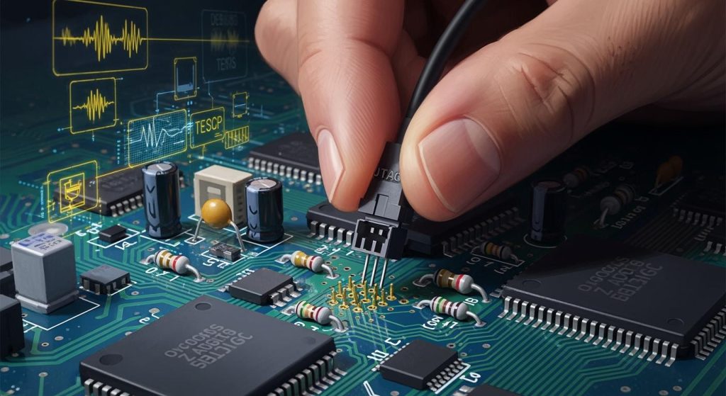
Early DFM reports can suggest setting test points on the PCB to test the circuit’s conductivity after all components are soldered. If possible, program burning can be carried out on the main control IC using burners like ST-LINK or J-LINK. This enables engineers to directly observe functional changes from various touch actions, verifying the functional integrity of the entire PCBA.
7. PCBA Board Testing
For orders requiring PCBA testing, the following tests may be performed:
- ICT (In Circuit Test)
- FCT (Function Test)
- Burn-In Test (Aging Test)
- Temperature and Humidity Test
- Drop Test
These tests should follow the customer’s test plan, and the report data can be summarized for analysis.
By integrating wonderfulpcb DFM Services into these key stages, hardware engineers can ensure that their designs are optimized for manufacturability and assembly, thus improving production efficiency, reducing costs, and minimizing the risk of errors throughout the manufacturing process.