In computer memory modules and graphics cards, there is a row of golden conductive contact pads, commonly known as “gold fingers.” In the PCB design and manufacturing industry, the PCB gold finger (Gold Finger or Edge Connector) refers to the connector used as the external interface for the PCB to connect to external devices. In this article, we will explore the design of the “gold finger” in PCB and discuss some key manufacturing considerations.

Functions and Applications of Gold Finger
Interconnect Point for Gold Finger When auxiliary PCBs (such as graphics cards or memory modules) connect to a motherboard, they do so through a slot, such as PCI, ISA, or AGP. The gold finger serves as the interconnection point, allowing the transmission of signals between the peripheral devices or internal cards and the computer.
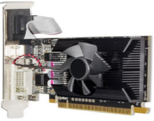
Special Adaptors, Gold fingers, can enhance the functionality of a motherboard by allowing a secondary PCB to be inserted into it. For example, memory, graphics cards, sound cards, network cards, and other cards connect via these edge connectors. These connections help transmit high-quality graphics and sound. Since these cards are rarely removed or reinserted, the gold finger is typically more durable than the card itself.
External Connection via Gold Finger External peripherals like speakers, subwoofers, scanners, printers, and displays are connected to the motherboard via the PCB “gold finger.” These peripherals are plugged into specific slots on the back of the computer, such as HDMI, DisplayPort, VGA, or DVI, which in turn connect to the motherboard’s PCB.
Manufacturing Design Considerations for PCB Gold Fingers
Design of the Gold Finger Bevel
- Safe Distance from Edge: The distance between the gold finger and the PCB’s edge should be considered based on the board’s thickness and the bevel angle of the “gold finger.” A common bevel angle is 45 degrees.
- If the gold finger is placed too close to the board edge and copper exposure is undesirable, adjustments should be made to ensure a safe distance between the gold finger and the PCB edge to avoid cutting into the copper.

Soldermask Window Design
- To facilitate card insertion, the gold finger area should have an opening in the soldermask. If not, soldermask ink between the gold fingers may chip off during repeated insertions, preventing good contact with the slot.
- The window for the gold finger or tin finger area should be opened slightly larger than the PCB edge (approximately 10 mils).
- The window should also be larger than the trace by 4 mils on one side. Be careful not to expose copper when opening the window; otherwise, copper should be removed.
- No windows should be made around the gold finger if the via is smaller than 2 mm.
Edge Processing for Board Corners
- To facilitate card insertion, the PCB outline near the gold finger should have beveled corners. Whether to use beveled or rounded corners depends on design preferences. If corners are not beveled, the right angle may damage the card slot during insertion and extraction, reducing the product’s reliability.
Copper Layer Design for Traces
- For ease of insertion, it’s best not to apply copper on the outer surface of the gold finger area. If multiple networks use the same trace, the copper layer might connect multiple gold fingers, making it difficult to insert or extract cards.
Design of Long and Short “Gold Fingers”
- For long and short gold fingers, the main trace should be 40 mils, the secondary trace 20 mils, and the connecting points 6 mils. The distance between the “gold finger” pad and the 20 mil trace should be 8 mils.
- When the main trace enters the board, it should be routed using diagonal lines. If there is a large notch near the gold finger, the traces should have rounded corners instead of sharp angles.
Panelization Design
- If the gold finger board size is smaller than 40×40 mm, the bevel should be processed first, followed by the milling of the PCB outline. CAM should design positioning holes at both ends of the PCB for secondary positioning. The automated bevel should ensure that the gold finger width is at least 40 mm.
- When penalizing, the gold finger should be oriented outward, with gold fingers facing inward to facilitate the addition of electrical gold leads.
Manufacturing Process of “Gold Finger” PCB
Process for Creating “Gold Fingers”
The process for creating “gold fingers” involves several steps:
- Material preparation
- Inner-layer imaging
- Inner-layer etching
- Inner-layer AOI (Automated Optical Inspection)
- Brown oxidation (baking)
- Lamination
- Drilling
- Copper plating
- Board electroplating
- Outer-layer imaging
- Graphic electroplating
- Outer-layer etching
- Outer-layer AOI
- Soldermask printing
- Soldermask imaging
- Soldermask inspection
- Character printing
- Soldermask second printing
- Soldermask second imaging
- Gold plating
- Electroplating the gold fingers
- Surface QC inspection
- Film removal
- Outer-layer imaging (second pass)
- Development (second pass)
- Outer-layer etching (second pass)
- Film stripping
- Milling
- Beveling of gold fingers
- Electrical testing
- Final inspection
- Shipping
CAM Compensation
- For multi-layer PCBs with gold fingers, the inner-layer copper thickness near the gold finger area should be 80 mils for standard products and 40 mils for optical or memory products.
- For designs without gold fingers, but where beveling is required, the copper layer must also follow the same rules as for gold fingers.
- The trace width for the gold finger leads should be 12 mils, with the current capacity of the gold finger being 40 mils.
- For optical products using a gold finger process (gold plating + edge connectors), no compensation is applied to the pad traces. The distance from the gold finger to the edge of the PCB should be at least 0.5 mm. If the board thickness tolerance is +/- 0.1 mm, copper should be added in the space around the gold finger area to facilitate penalization, and non-metallic holes of 0.4 mm should be added at the corners of the “gold finger” section.