PCB flatness standards are very important for good performance. Bow and twist are ways a printed circuit board can bend. Bow is when the board curves along its length. Twist is when the corners are at different heights. These problems can make assembly hard and hurt how the pcb works. IPC-6011 standards say circuits should be balanced and built the same on both sides. This helps stop bow and twist. When copper weights are 3 oz/ft² or more, stricter rules are needed. Flatness control keeps the pcb steady and stops the need for extra support parts.
Bow and twist change how flat a pcb is and decide if the printed circuit board will pass tough industry rules.
Key Takeaways
Bow and twist make PCBs bend, which can hurt how they work. It is important to control bow and twist. – Using IPC-TM-650 tools checks flatness early. This helps find problems fast and makes sure boards follow the rules. – Making PCBs with even copper and smart part spots helps stop bow and twist when making them. – Picking good materials and the right thickness keeps PCBs strong. This makes them less likely to bend from heat or water. – Talking well between makers and customers helps fix problems faster and makes PCBs better.
PCB Flatness Standards
Bow and Twist
PCB flatness means how smooth and even the board is. Bow and twist are the main ways a board can lose flatness. Bow happens when all four corners touch the table, but the middle rises up. Twist is when three corners touch, but one corner is higher or lower. These problems can show up during making the board, especially after heating steps. Bow can be as much as 0.47 mm, and it changes with board material and heat. Twist is when the board turns along its diagonal, so one corner is up or down.
Bow and twist do not follow a normal pattern. Different materials and heat during soldering cause these changes. People use special ways to check bow and twist. They look at the board, use flatness tools, and sometimes 3D scanning. Rules like IPC-TM-650 2.4.22 explain how to measure and accept boards for bow and twist.
The table below shows the most bow and twist allowed for each board type:
Board Type | Maximum Bow and Twist (%) |
|---|---|
With Surface Mount Devices | 0.75% |
Without SMD | 1.5% |
These limits come from IPC 2422-1 and IPC 2422-2 rules. They make sure boards work well, even if they bend a little.
Why Flatness Matters
Flatness is very important for how well a pcb works. Bow and twist can make it hard to put parts on the board. If the board is not flat, parts may not fit right, and solder may not stick well. This can cause open circuits or weak spots.
Studies show flat pcbs last longer and work better. Too much bow or twist puts stress on solder joints. How you fasten the board, like where you put bolts, changes how much it bends. Bolts far from important parts help solder joints last longer. If bolts join the pcb to things that expand differently with heat, solder joints can break up to 60% sooner. Tests and computer models show that support plans change where cracks start and how long solder joints last.
Researchers found that flatter pcbs give better results in making boards. Boards with less coplanarity have fewer solder problems. For example, at 0.177 mm coplanarity, the chance of a solder open is about 1%. Boards that pass tests are usually flatter than ones that fail. Where the board sits on the panel and how it breaks off also matter, but copper balance and material do not change things much.
Bow and twist control is not just about following rules. It helps every printed circuit board work well and last longer in real life.
Measurement Methods
IPC-TM-650
Engineers use different ways to check how flat a printed circuit board is. The IPC-TM-650 standard explains how to test for bow and twist. To do this, you put the board on a flat surface. Then you measure the highest and lowest spots. People use tools or special cameras for this. Some common tools are shadow moiré, fringe projection, and confocal measurement. These tools can find very small height changes, sometimes as tiny as 5 micrometers. Some designers want even more exact checks, like 1 or 3 micrometers.
To measure flatness, you must follow some steps:
Bake the board first to get rid of water.
Paint the board white so cameras can see better.
Cut the board so it fits in the oven.
Put thermocouples close to, but not in, the test area.
Use heat that goes up slowly, between 0.5°C and 1.0°C each second.
The IPC-TM-650 standard also says to check big panels before cutting them into smaller boards. This makes sure all boards are good before putting them together.
Acceptable Limits
There are clear rules for how flat a board should be. The right numbers depend on what kind of board it is and how it will be used. The table below shows the main limits:
Board Type | Bow and Twist Limit (%) |
|---|---|
Surface mount printed circuit boards | 0.75 |
Other board types | 1.5 |
Boards also have to be the right thickness and have smooth edges. If a board is thicker than 31 mils, it must be within ±10% of the right thickness. Thinner boards can only be off by ±3 mils. If a board bends more than 0.75%, it is not okay for most jobs. These rules help make sure boards work well when being made and used.
By following these bow and twist tests, companies can make boards that meet the rules and do not fail as much.
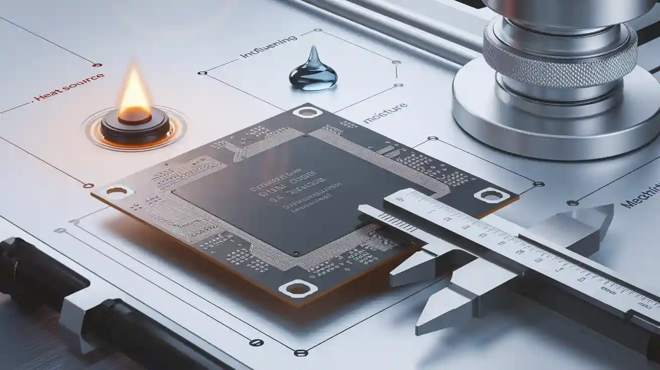
Influencing Factors for PCB Flatness
Design and Layout
How you design and lay out a pcb changes how flat it stays. Engineers try to keep copper even on both sides. If one side has more copper, the board can bend. This happens when the board cools down. A balanced stack-up helps stop this problem. Traces and planes are placed to spread out stress. Big cutouts or slots can make weak spots. These weak spots make bow or twist more likely during lamination. Where you put parts and holes also matters. Good choices in design help stop bending. This makes the pcb work better and last longer.
Tip: Keeping copper even and putting parts in smart spots helps stop bow and twist when making a circuit board.
Materials and Thickness
The materials and thickness you pick decide how flat the pcb will be. Different materials act differently with heat and water. FR4, Teflon, and flexible substrates each have special traits. FR4 has a medium CTE, but Teflon’s CTE is much higher. Flexible substrates need extra care to stay flat. When these materials get hot during lamination, they grow and shrink at different speeds. This can make the board bend or twist.
How thick the board is also matters a lot. Thin boards bend or twist more easily. Thick boards do not bend as much but can be too stiff. The table below shows how material and thickness change flatness and tolerance:
Parameter | Description | Impact on PCB Flatness and Tolerances |
|---|---|---|
Material Type | FR4, Teflon, Flexible Substrates | Different CTEs make boards warp or shrink; Teflon is harder to keep flat, flexible substrates need special care |
Thickness Range (mm) | 0.2–0.4 | ±0.1mm tolerance; thick boards lose flexibility, thin ones are weak |
Thickness Range (mm) | 0.5–1.0 | ±0.2mm tolerance; thick boards slow high-speed signals, thin ones are not stable |
Thickness Range (mm) | 1.0–1.5 | ±0.3mm tolerance; thick boards are hard to mount, thin ones can break |
Thermal Expansion Effects | FR4 (14-16 ppm/°C), Teflon (30-40 ppm/°C), Polyimide (10-20 ppm/°C) | Higher CTE means more warping, which hurts flatness |
Environmental Factors | Temperature, Humidity | Heat and water make boards grow, shrink, or warp |
Manufacturing Processes | Reflow soldering thermal stress | Uneven cooling bends boards and moves parts |
Engineers pick materials and thickness based on what the pcb needs. They also think about how these choices change bow and twist during making and using the board.
Layer Count
The number of layers in a pcb changes how much it bends. More layers mean more lamination steps. Each step uses heat and pressure. These steps can make the board bend or twist if not balanced. More layers can mean more stress. If layers are not the same thickness or type, the board can bend after lamination.
Designers use even stack-ups to help with this. They match layers above and below the middle. This keeps the board flat during making. If the stack-up is not even, the board can bend during lamination. Planning the number of layers and stack-up helps stop bow and twist.
Manufacturing Process
How the pcb is made changes how flat it is at the end. Every step, like lamination and soldering, can cause problems. Lamination uses heat and pressure to stick layers together. If heat or pressure is not even, the board can bend. Cooling that is not even after lamination also causes bending. During reflow soldering, the board gets hot again. This heat can make the board bend, especially if materials grow at different rates.
Manufacturers use careful steps to stop these problems. They watch heat and pressure during lamination. They bake boards before soldering to dry them out. These steps help stop bow and twist. Teams check flatness many times during making. Early checks find problems before the next step. Good control of the process keeps the pcb flat and lowers the chance of problems.
Note: Keeping the process steady during making and lamination is very important to stop bow and twist in every pcb.
Ensuring PCB Compliance
Best Practices
Manufacturers use different ways to keep pcb flatness. They pick surface finishes like ENIG or ENEPIG. These finishes help pads stay even and strong. Dry film solder masks can make boards very flat, down to 5-7 micrometers. Engineers design stack-ups that are the same on both sides. They balance copper to stop bow and twist. Empty copper spots get filled to keep plating even. During lamination, they watch heat and pressure to stop warping. The table below lists some important numbers:
Aspect | Details / Numerical Benchmarks |
|---|---|
IPC Warpage Limits | 0.1% for Class 3 boards; 0.05% for Class 4; 0.2% for Class 1 |
Core Thickness | 1.6 mm helps big panels stay stiff if over 400 mm |
Copper Distribution | Balanced copper lowers warping risk by 15-20% |
Material Selection | High-Tg FR-4 (>170°C) or polyimide (up to 260°C) cuts expansion by about 20% |
Tip: Working with fabricators early and making quick test boards can find up to 80% of flatness problems before making lots of boards.
Manufacturer-Customer Communication
Good communication between makers and customers helps pcb compliance. Both sides should agree on flatness rules before making boards. Sharing stack-up plans, material picks, and lamination steps stops surprises. Makers can show computer tests to explain how the pcb will act during assembly. Customers should tell makers about any problems found in testing. This teamwork helps improve both design and making steps.
Regular meetings keep everyone updated.
Sharing test results and samples helps fix things fast.
Talking about problems in making leads to quicker fixes.
Addressing Issues
When flatness problems show up, teams follow steps to fix them. First, they check if copper is balanced and stack-up is even. Next, they see if the right materials and thickness were used. If lamination or soldering caused the problem, they change the process settings. Sometimes, they use special holders during assembly to keep boards from bending. Case studies show that trying new designs or changing how parts attach can fix hard problems. For example, a European sensor project got better flatness by testing three new designs. This helped them make more boards. In medical devices, making many test boards and getting design help led to better results and stronger boards.
Teams that find problems early and improve their process have fewer flatness issues and better pcb performance.
Knowing PCB standards and what affects quality helps engineers make good products. Good design, picking the right materials, and careful steps stop boards from bending. This also helps put parts on the board better. The table below shows two ways to cut boards apart. It tells how each way changes the edge and stress:
Aspect | Stamp Hole Depaneling | V-Scoring Depaneling |
|---|---|---|
Processing Cost | Cheap and easy to do | Expensive and needs more work |
Depaneling Quality | Edges are rough and need to be trimmed | Edges are smooth and look nice |
Depaneling Stress | Not much stress, good for fragile parts | Lots of stress, so parts need protection |
Design Flexibility | Works for many shapes and designs | Only works for simple, regular shapes |
Suitable Scenarios | Good for small jobs and test boards | Best for making lots of boards that must be flat |
For more help, check IPC-6012 and IPC-2221 rules. Checking boards often and working together helps everyone get better results.
FAQ
What causes a PCB to lose flatness?
Many things can make a PCB not flat. If copper is not spread out evenly, the board can bend. Picking the wrong materials also makes problems. Heat during making the board can cause bow or twist. Designers and makers must watch these things to keep the board flat.
How do engineers measure PCB flatness?
Engineers use special tools to check flatness. Some tools are shadow moiré, fringe projection, and confocal measurement. They follow rules from IPC-TM-650. The board goes on a flat table. Then they check the highest and lowest spots. This helps make sure the board is good enough for use.
What happens if a PCB fails flatness standards?
If a PCB is not flat enough, it can cause trouble. Parts may not fit right on the board. Solder joints can get weak and break. This might make the board stop working or not last long. Makers must fix the problem before using the board.
Can design changes improve PCB flatness?
Yes, design changes can help keep boards flat. Engineers balance copper layers and pick good materials. They plan the stack-up to be even. They do not use big cutouts and put parts in smart places. These steps help stop bow and twist when making the board.