01
What is PCB surface treatment process?
Copper surfaces on PCB without solder mask coverage, such as solder pads, gold fingers, mechanical holes, etc. If there is no protective coating, the copper surface is easily oxidized, which affects the soldering between bare copper and components in the solderable area of the PCB.
As shown in the figure below, the surface treatment is located on the outermost layer of the PCB, above the copper layer, serving as a “coating” on the copper surface.
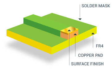
The main function of surface treatment is to protect the exposed copper surface from oxidation circuits, thereby providing a solderable surface for soldering during welding.
02
Classification of PCB surface treatment processes
PCB surface treatment processes are divided into the following categories:
Hot air solder leveling (HASL)
Tin immersion (ImSn)
Chemical nickel gold (immersion gold) (ENIG)
Organic Solderable Preservatives (OSP)
Chemical Silver (ImAg)
Chemical nickel plating, chemical palladium plating, immersion in gold (ENEPIG)
Electrolytic Nickel/Gold
Hot air solder leveling (HASL)
Hot Air Solder Level (HASL), commonly known as spray tin, is a surface treatment process that is most commonly used and relatively inexpensive. It is divided into lead-free spray tin and lead spray tin.
The shelf life of PCB can reach 12 months, with a process temperature of 250 ℃ and a surface treatment thickness range of 1-40um.
The tin spraying process involves immersing the circuit board in molten solder (tin/lead) to cover the exposed copper surface on the PCB. When the PCB leaves the melted solder, high-pressure hot air blows through the surface with an air knife, causing the solder to deposit flat and removing excess solder.
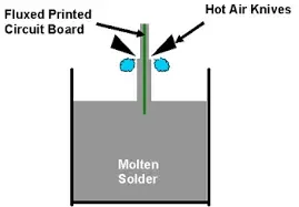
The process of tin spraying requires mastery of welding temperature, blade temperature, blade pressure, immersion welding time, lifting speed, etc. Ensure that the PCB is completely immersed in the melted solder, and the air knife can blow up the solder before it solidifies. The pressure of the air knife can minimize the meniscus on the copper surface and prevent solder bridging.
Hot air solder leveling (HASL)
advantage:
Long shelf life
Good weldability
Corrosion and oxidation resistance
Visual inspection is possible
Disadvantages:
Surface unevenness
Not suitable for devices with small spacing
Easy to produce tin beads
Deformation caused by high temperature
Not suitable for electroplating through holes
Tin immersion (ImSn)
Immersion Tin (ImSn) is a metal coating deposited through chemical displacement reaction, directly applied to the base metal (i.e. copper) of the circuit board, which can meet the requirements of small pitch components for PCB surface flatness.

Tin deposition can protect the underlying copper from oxidation during the 3-6 month shelf life. Since all solder is tin based, the tin deposition layer can match any type of solder. After adding organic additives to the tin immersion solution, the tin layer structure becomes granular, overcoming the problems caused by tin whiskers and tin migration, while also having good thermal stability and weldability.
The temperature of the tin deposition process is 50 ℃, and the surface treatment thickness is 0.8-1.2um. PCB that is particularly suitable for connection through crimping, such as communication backboards.
Tin immersion (ImSn)
advantage:
Suitable for small spacing/BGA
Good surface smoothness
Compliant with RoHS
Good weldability
Good stability
Disadvantages:
Easy to be contaminated
Tin whiskers may cause short circuits
Electrical testing requires soft probes
Not suitable for contact switches
Corrosive to solder mask layer
Chemical nickel gold (immersion gold) (ENIG)
Chemical Nickel Immersion Gold (ENIG) can meet the surface flatness and lead-free processing requirements of PCB for small pitch devices (BGA and μ BGA).
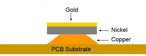
ENIG consists of two layers of metal coatings, with nickel deposited on the copper surface through chemical processes and then coated with gold atoms through displacement reactions. The thickness of nickel is 3-6 μ m, and the thickness of gold is 0.05-0.1 μ m. Nickel acts as a barrier to copper and is the surface to which the components are actually soldered. The role of gold is to prevent nickel oxidation during storage, with a shelf life of about one year, and can ensure excellent surface flatness.
The immersion gold process is widely used in high-density boards, conventional hard boards, and soft boards, with high reliability and support for wire bonding using aluminum wire. Widely used in industries such as consumer, communication/computing, aerospace, and healthcare.
Chemical Nickel Gold (ENIG)
advantage:
Long shelf life
High density board (μ BGA)
Aluminum wire bonding
High surface flatness
Suitable for electroplating holes
Disadvantages:
expensive price
Attenuation of RF signals
Cannot rework
Black pad/black nickel
The processing process is complex
Organic Solderable Preservatives (OSP)
Organic Solderability Preservatives (OSP) are very thin material protective layers applied to exposed copper to protect the copper surface from oxidation.
Organic films have characteristics such as oxidation resistance, thermal shock resistance, and moisture resistance, which can protect copper surfaces from oxidation or sulfurization under normal conditions. In the post high temperature welding process, the organic film is easily removed by the flux, causing the exposed clean copper surface to immediately bond with the melted solder, forming a strong solder joint in a very short period of time.
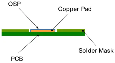
OSP is a water-based organic compound that can selectively bind with copper to protect the copper surface before welding. Compared with other lead-free surface treatment processes, it is very environmentally friendly because other surface treatment processes may have toxicity or higher energy consumption.
Organic Solderable Preservatives (OSP)
advantage:
Simple and cheap
Lead free environmental protection
Smooth surface
Wire bonding
Disadvantages:
Not suitable for PTH
Short shelf life
Not convenient for visual and electrical inspection
ICT fixtures may damage PCB
Chemical Silver (ImAg)
Immersion silver (ImAg) is a process of directly plating copper with a layer of pure silver by immersing a PCB in a silver ion bath through displacement reaction. Silver has stable chemical properties. PCB processed through silver immersion technology can maintain good electrical and solderability even when exposed to hot, humid, and polluted environments, and even if the surface loses its luster.
Sometimes, to prevent silver from reacting with sulfides in the environment, silver deposition is combined with OSP coating. For most applications, silver can replace gold. If you do not want to introduce magnetic materials (nickel) into the PCB, you can choose to use silver deposition.
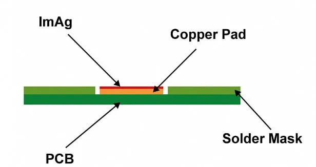
The surface thickness of silver deposition is 0.12-0.40 μ m, and the shelf life is 6 to 12 months. The silver deposition process is sensitive to the cleanliness of the surface during processing, and it is necessary to ensure that the entire production process does not cause surface contamination of the silver deposition. The silver deposition process is suitable for applications such as PCB, thin-film switches, and aluminum wire bonding that require EMI shielding.
Sinking Silver (ImAg)
advantage:
Good surface flatness
High weldability
Good stability
Good shielding performance
Suitable for aluminum wire bonding
Disadvantages:
Sensitive to pollutants
Easy to undergo electromigration
Silver metal whiskers
Short assembly window after unpacking
Difficulty in electrical testing
Chemical nickel plating, chemical palladium plating, immersion in gold (ENEPIG)
Compared with ENIG, ENEPIG has an additional layer of palladium between nickel and gold, which further protects the nickel layer from corrosion and prevents possible black pads during ENIG surface treatment, thus providing an advantage in surface smoothness. The deposition thickness of nickel is about 3-6 μ m, the thickness of palladium is about 0.1-0.5 μ m, and the thickness of gold is 0.02-0.1 μ m. Although the thickness of the gold layer is thinner than ENIG, it is more expensive.
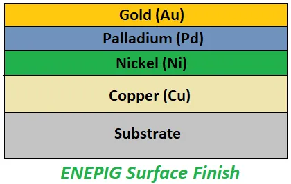
The layer structure of copper nickel palladium gold can be directly wire bonded to the plating layer. The last layer of gold is very thin and soft, and excessive mechanical damage or deep scratches may expose the palladium layer.
Chemical nickel plating, chemical palladium plating, immersion in gold (ENEPIG)
advantage:
Extremely flat surface
Wire bonding
Can be reflow soldered multiple times
High reliability of solder joints
Long shelf life
Disadvantages:
expensive price
Gold wire bonding is not as reliable as soft gold bonding
Easy to produce tin beads
Complex process
Difficult to control the processing process
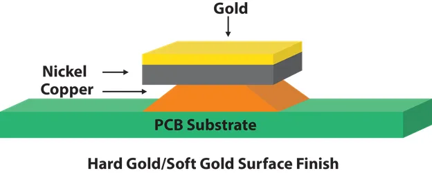
Electrolytic Nickel/Gold
Electroplated nickel gold is divided into “hard gold” and “soft gold”.
Hard gold has a low purity (99.6%) and is commonly used for gold fingers (PCB edge connectors), PCB contacts, or other hard wear areas. The thickness of gold can vary according to requirements.
Soft gold is purer (99.9%) and is commonly used for wire bonding.
Hard electrolytic gold
Hard gold is a gold alloy containing cobalt, nickel, or iron complexes. Low stress nickel is used between gold plating and copper. Hard gold is suitable for components that are frequently used and highly likely to wear out, such as carrier boards, gold fingers, and key pads.
The thickness of hard gold surface treatment may vary depending on the application. The recommended maximum weldable thickness for IPC is 17.8 μ in, 25 μ in gold and 100 μ in nickel for IPC1 and Class 2 applications, and 50 μ in gold and 100 μ in nickel for IPC3 applications.
Soft electrolytic gold
Mainly used for PCB that require wire bonding and high solderability, soft gold soldering joints are more secure compared to hard gold.
Soft electrolytic gold surface treatment
Electrolytic Nickel/Gold
advantage:
Long shelf life
High reliability of solder joints
Durable surface
Disadvantages:
Very expensive
Gold finger requires additional conductive wiring on the board
Hard gold has poor weldability
03
How to choose PCB surface treatment process?
The surface treatment process of PCB will directly affect the output, rework quantity, on-site failure rate, testing capability, and scrap rate. For the quality and performance of the final product, it is necessary to choose a surface treatment process that meets the design requirements. In engineering, the following perspectives can be considered:
Pad flatness
The flatness of solder pads directly affects the soldering quality of PCBA, especially when there are relatively large BGA or smaller pitch μ BGA on the board, ENIG, ENEPIG, and OSP can be selected when the protective layer on the solder pad surface needs to be thin and uniform.
Solderability and Wettability
Solderability is always a key factor for PCB. While meeting other requirements, it is advisable to choose a surface treatment process with high solderability to ensure the yield of reflow soldering.
Welding frequency
How many times do PCB need to be soldered or reworked? The surface treatment process of OSP is not suitable for rework more than twice. At this time, composite surface treatment processes such as immersion gold+OSP will also be chosen. Currently, high-end electronic products such as smartphones will choose this treatment process.
RoHS compliance
The lead element in PCBA mainly comes from component pins, PCB pads, and solder. In order to comply with ROHS regulations, the surface treatment method of PCB must also comply with ROHS standards. For example, ENIG, tin, silver, and OSP all comply with ROHS standards.
Metal bonding
If gold or aluminum wire bonding is required, it may be limited to ENIG, ENEPIG, and soft electrolytic gold.
Reliability of solder joints
The surface treatment process of PCB can also affect the final soldering quality of PCBA. If high reliability solder joints are required, the use of immersion gold or nickel palladium gold process can be chosen.