Meeting strict 5G base station PCB design rules helps you make strong networks. You face new problems with 5G PCB design that make it different from older types. Faster signals and tricky layouts need better materials and new ways to build.
The dielectric constant for materials in 5G PCBs can go as low as 3, but older ones used higher numbers.
Fast signals make more heat, so you need materials that move heat away well.
You must use inspection tools to find risks that could hurt signal quality.
You need real solutions to pick the best materials and design plans for 5G Base Stations.
Key Takeaways
Pick materials that have low dielectric constants and high thermal conductivity. This helps signals stay strong in 5G PCBs.
Make PCBs with many layers. This helps handle lots of paths and keeps signals clear. It also lowers interference.
Use special inspection tools to find problems early. This makes sure 5G PCB manufacturing is high quality and reliable.
Test PCBs in tough environments and check reliability. This makes sure they work well in hard conditions and keep performing.
Follow strict design rules for impedance control and crosstalk reduction. This helps signals stay good in 5G uses.
5G Base Station PCB Requirements
High-Frequency and Signal Integrity
You have to follow strict 5g pcb design rules for high-frequency signals in 5g base stations. These stations use phased array antennas and beamforming to send signals exactly where needed. This helps you get better coverage and less interference in new communication systems. High-frequency signals let you send lots of data fast, but keeping the signal clear is harder.
You must pick materials and layouts that stop signal loss. The 5g pcb design should keep signals strong and clear as they move through the 5g circuit board. If you do not control impedance and crosstalk, you can lose bandwidth and lower how well advanced 5g applications work. Careful routing and stack-up planning help you meet 5g pcb design rules for signal integrity.
Layer Count and Dense Routing
5g base stations need complex 5g pcb design with many layers. You often need 10 to 16 copper layers for all the dense routing needed for fast data. Each layer has different signal paths, power planes, and ground planes. This setup helps you keep signals apart and cut down on interference.
Dense routing is very important for 5g pcb design. You have to fit many traces in a small space without causing signal trouble. The 5g circuit board must handle both analog and digital signals for 5g technology. You need to plan so each signal path is short and direct. This helps you keep signal loss low and signal quality high for all channels.
Environmental and Reliability Demands
Outdoor 5g base communication stations face tough weather. Your 5g pcb design must handle heat, cold, humidity, and vibration. If you do not plan for these, the 5g circuit board might break or not work well.
Tip: Pick materials that move heat away from hot parts. This keeps your pcb safe when it runs at high power.
You should also make sure your 5g pcb design uses materials that stay strong in changing weather. Humidity can hurt how well your pcb works. Mechanical stability is important to keep electrical performance steady when the weather changes.
Your 5g pcb design rules should include:
Heat control for both outside and inside sources
Steady electrical and mechanical properties
Protection from humidity and moisture
Strong mechanical stability when there is vibration and temperature change
You must also follow strict reliability rules for 5g base stations. The table below shows some common needs for long-term use:
Aspect | Details |
|---|---|
Raw Material Control | Weather-resistant coatings (immersion gold thickness ≥0.8μm) and high-stability substrates (Tg=170℃). No surface corrosion area exceeds <5% after a 2000-hour salt spray test (NSS standard). |
In-Process Inspection | LDI laser imaging with ±2μm positioning accuracy and AOI+AXI dual inspection technology keep defect rates below 0.03%. |
Reliability Verification | Passed 1000-hour 85℃/85%RH damp heat test and 5000 cycles of -40℃~85℃ temperature cycle test with a variation rate of main parameters <5%. |
Meeting these rules makes sure your 5g base stations give reliable communication for advanced 5g applications. You support the high needs of 5g technology and help build strong networks for the future.
Material Selection for 5G PCB Design
Picking the right materials for your 5g base station PCB is very important. These materials must help fast signals and survive outside. You need to think about both high-frequency needs and tough weather.
Substrate and Laminate Choices
Start by choosing substrates and laminates that keep 5g signals clear. The table below lists the main types and what they do:
Material Type | Key Properties | Applications |
|---|---|---|
Substrates | Dielectric constant consistency, moisture resistance, mechanical stability | Foundation for PCBs, crucial for signal integrity |
Controlled impedance, reduced crosstalk | Miniaturization and multi-layer designs | |
Laminates | Low coefficient of thermal expansion, signal speed, multi-layer compatibility | Core layers in high-density 5g PCBs |
You want materials that do not change shape in heat or wet weather. This helps your 5g circuits work well all the time.
Dielectric and Loss Properties
For 5g, you need materials with a low dielectric constant and low loss tangent. These things help signals move fast and not lose power. If you use a material with high loss tangent, like FR4, signals can turn into heat. Rogers materials have a loss tangent as low as 0.001. They keep your data safe and clear.
Low dielectric constant keeps signals fast.
Low loss tangent means less energy is lost.
High thermal conductivity moves heat away from busy circuits.
Tip: Always check both dielectric and thermal properties before picking a material for your 5g PCB.
UV, Pollutant, and Temperature Resistance
Your 5g base station PCBs face sun, rain, and pollution. You need materials that block UV light, chemicals, and big temperature changes. Polyimide films can handle strong UV for over 1,000 hours. Some materials work from -40°C to 85°C. High thermal performance is needed for outdoor 5g stations.
Polycarbonate is light and strong, so it is easy to install.
These materials do not soak up water and stay strong in heat.
High thermal conductivity laminates help control heat from 5g circuits.
If you pick good materials, your 5g base station will last longer and work better, even in bad weather.
5G PCB Design and Layout Guidelines
Stack-Up and Routing Strategies
You need a good plan for your stack-up in 5g pcb design. Put high-frequency signal planes next to ground planes. This helps keep signals clear and steady. Place power planes close to ground planes for better decoupling. Use low-Dk materials like Rogers RT/duroid 5880 for better high-frequency work. Give some layers just to ground and power for more stability. Put low-frequency signals on layers that are not as important. Try using 45-degree angles when routing traces to stop reflections. Keep high-speed parts close to connectors to make traces short. Controlled impedance routing stops signals from bouncing and getting mixed up.
Phased Array and Beamforming Integration
Phased array antennas use many radiating parts in special patterns. Each part connects to a delay line or phase shifter. This lets you make a beam that does not spread out much. You must match feedline lengths inside and between antenna groups. There are two main types: discrete patch antennas and parallel arrays. Your design should have impedance transformer sections for best power transfer and radiation.
Series-fed patches | Parallel patches |
|---|---|
Gain goes up with more patches | Gain can be limited by feedline losses |
Fewer patches give lower gain | More feedline losses happen |
Narrow impedance bandwidth | Wide impedance bandwidth |
Smaller feedlines help stop sidelobes | Feedline emissions can make sidelobes |
Beamforming makes 5g pcb design harder. You need special materials for 5g frequencies. It is very important to manage heat and keep signals strong. Even small mistakes can lower how well it works.
EMI/EMC and Signal Integrity
You must control EMI and EMC in 5g pcb design. A good stack-up helps stop electromagnetic interference. Keep layers close together, like 0.12 mm between signal and ground, to lower signal loss. Good layout helps you make loop areas small and route high-speed signals safely. Use common-mode chokes and ferrite beads to block high-frequency noise. Metal enclosures can shield signals but may make the board heavier. Differential signaling works better but needs careful space planning.
Signal integrity depends on ground planes and how you route differential pairs. Controlled impedance traces stop signals from bouncing back. Short traces help lower electromagnetic interference. Keep digital and analog parts apart for better isolation.
Crosstalk and Trace Optimization
Crosstalk is worst when two traces run side by side. Make parallel traces as short as you can to lower crosstalk.
Buried via designs help cut signal loss from stub effects. This keeps signals strong at high frequencies like 28 GHz. Make space between signal traces at least three times the trace width. Use ground planes and guard traces to soak up unwanted signals. Put signal layers next to ground or power planes for better shielding. Route differential pairs together with even spacing and do not run them next to other fast signals.
High-density interconnect pcbs are used a lot in 5g. These designs make signal paths shorter and lower delay. Controlled impedance and good grounding stop reflections and electromagnetic interference. Short, direct traces are best for RF and high-speed digital signals. This way, you lose less power and get better performance.
5G PCB Manufacturing Process
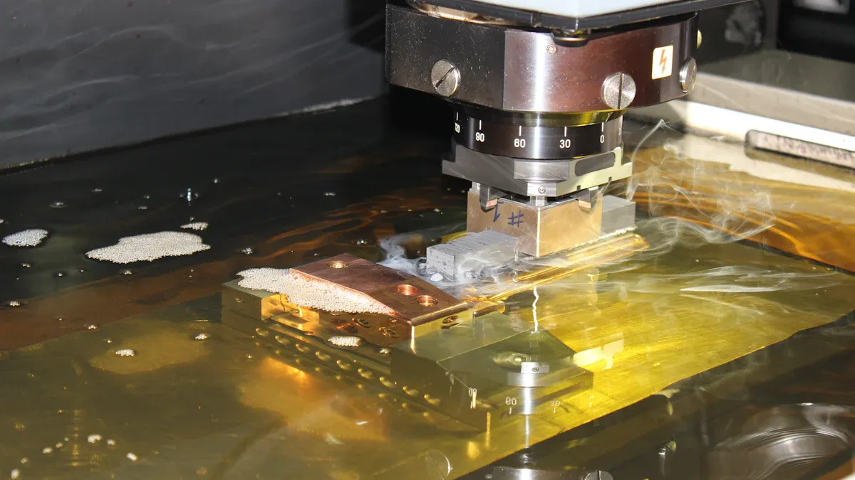
Large-Panel and Real-Time Adaptability
When you make big panels for 5g base stations, you need special steps. Impedance control is very important for these panels. You must keep the signal strength steady for high-frequency signals. Modeling tools like Polar Si9000 help you check if your panel is good. Ceramic substrates, like aluminum nitride, help move heat away and keep signals clear. Sputtering and electroplating add metal layers to the board. These methods let you make thin lines for fast signals. Laser-drilled vias connect layers without hurting the board. You have to plan how many layers you need for all your signals and pins. Work with your material suppliers to make sure everything fits your 5g needs. Always check your materials before you start to see if they meet IPC rules.
Real-time adaptability helps you keep your 5g pcb process working well. The table below shows how new technology helps you:
Benefit | Description |
|---|---|
Defect Prediction | Machine learning finds where defects might happen. |
Process Optimization | AI changes settings to keep quality high. |
Yield Enhancement | Analytics spot problems early, so you can fix them fast. |
Improvement Statistics | Companies see 15-30% better yield and 50% less rework. |
Advanced Inspection and Imaging
You need advanced inspection tools to keep your 5g pcb quality high. Direct Imaging (DI) helps you control impedance and make boards with many layers. Automated Optical Inspection (AOI) checks very small lines, even down to 5 microns. This is important for fast 5g systems. Automated Optical Shaping and Repair lets you fix tiny problems quickly. You can see the main tools in the table below:
Technology | Application in 5G PCB Manufacturing |
|---|---|
Direct Imaging (DI) | Keeps impedance tight and helps with high-layer boards. |
Automated Optical Inspection (AOI) | Checks fine lines for errors in 5g systems. |
Automated Optical Shaping and Repair | Repairs opens and shorts in high-density boards. |
AOI and X-ray inspection can find more than 99% of problems. Finding problems early saves you money and time. X-ray inspection finds hidden problems, like holes in solder joints. When you use both AOI and X-ray, you can lower problems to less than 1%.
Quality Control and Yield Management
You must follow strict quality control steps for 5g pcb manufacturing. The table below shows what you need to check:
Quality Control Measure | Description |
|---|---|
Material Verification Testing | Checks dielectric constants and loss tangents for all frequencies. |
Advanced Dimensional Inspection | Makes sure all sizes are correct to the micron. |
Specialized RF Testing | Uses S-parameter and group delay tests for high-frequency signals. |
Environmental Stress Testing | Combines heat and RF tests to check real-world strength. |
Statistical Process Control (SPC) | Watches key numbers to keep everything in control. |
Machine Learning Algorithms | Finds small changes before they cause big problems. |
You also need to check for Dk deviation, Df (loss tangent), and thickness. Keep Dk at or below ±0.1 and Df below 0.003. Make sure there are no bubbles, delamination, or scratches. Use pure copper and the right amount of resin for strong bonding. Automated Optical Inspection now uses better cameras and pattern tools. Electrical tests use Vector Network Analyzers and Time Domain Reflectometry for high-frequency checks. Special fixtures help you test mmWave signals.
Tip: Good quality control keeps your 5g pcb strong and helps you reach all your design goals.
Testing and Validation for 5G PCBs
RF and Performance Testing
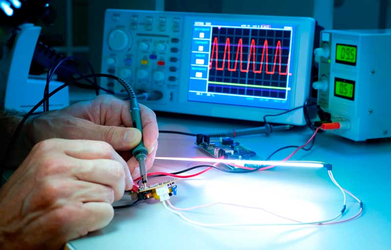
You need to make sure your 5g pcb works well before you use it in the field. RF and performance testing help you check if your design meets all the needs for fast signal transmission. You use special tools and steps to measure how well your 5g circuit design testing works.
Use a Vector Network Analyzer (VNA) to measure S-parameters. This shows how signals move through your pcb and if there is any loss or reflection.
Test the antenna pattern inside an echoic chamber. This helps you see if your 5g signals go in the right direction and reach far enough.
Build prototypes for testing before you make the full batch. This lets you find problems early and fix them.
You should avoid mistakes like mixing digital and RF grounds, skipping impedance control, or picking the wrong material for high-frequency transmission. These errors can hurt your signal quality and lower performance.
Environmental and Reliability Testing
You want your 5g pcb to last a long time, even in tough places. Environmental and reliability testing checks if your board can handle heat, cold, moisture, and shaking. These tests show if your pcb will keep working when the weather changes or during transport.
Test | Range |
|---|---|
Temperature cycling | -55°C to +150°C |
Thermal shock | Rapid transitions |
Humidity (85/85) | Moisture reliability |
Vibration Test | Simulates transportation conditions |
You run these tests to make sure your 5g board keeps its signal strength and does not break. Good testing helps you trust your pcb in real-world 5g networks.
Compliance with 5G Standards
You must check if your 5g pcb meets all the rules for 5g networks. Compliance testing covers many steps:
Field testing measures how your board works in real 5g networks. You see if the signal transmission stays strong.
Conformance testing checks if your pcb follows the standards set by groups like 3GPP.
Network stress testing pushes your board to its limits. You see how it handles heavy use and if the performance drops.
Note: Careful validation at every step helps you avoid problems later. You make sure your 5g circuit design testing gives you the best results for signal transmission and long-term use.
You can build strong 5G base station PCBs by following a few key steps.
Choose materials that support high-frequency signals and resist weather.
Plan your design to keep signals clear and reduce loss.
Use advanced inspection and testing to catch problems early.
Work with skilled PCB manufacturers. They help you meet 5G needs and deliver reliable networks.
FAQ
What materials work best for 5G base station PCBs?
You should use materials like Rogers, polyimide, or ceramic. These materials keep signals strong and resist heat, moisture, and sunlight. They help your PCB last longer outdoors.
How do you keep signal quality high in 5G PCBs?
You need to use controlled impedance routing and short, direct traces. Place ground planes close to signal layers. This setup reduces signal loss and keeps your data clear.
Why do 5G PCBs need so many layers?
You need more layers to fit all the fast signal paths, power planes, and ground planes. More layers help you separate signals and cut down on interference.
What tests should you run before using a 5G PCB?
You should run RF tests, temperature cycling, and humidity checks. Use a Vector Network Analyzer to measure signal loss. These tests show if your PCB works well in real conditions.