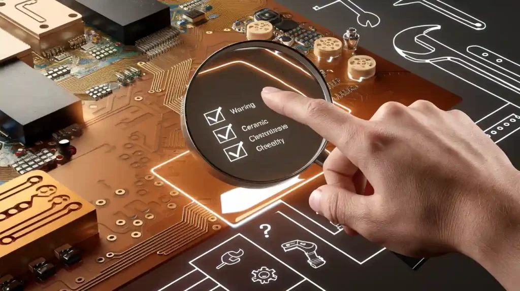
Power integrity simulation analytics play a vital role in ensuring reliable PCB designs. They help you analyze and optimize the power delivery network (PDN) to maintain stable voltage and current levels across your circuit. High-speed PCBs demand precise PDN impedance design to prevent ripple and noise, which can degrade performance. Addressing power integrity issues early allows you to predict behavior and experiment efficiently, saving costs compared to building multiple prototypes.
Neglecting power integrity can lead to serious consequences. Voltage drops may cause components to malfunction, while ground bounce can disrupt sensitive circuits. Poor power plane design or improper capacitor placement often results in voltage fluctuations, reducing signal integrity and device reliability.
Key Takeaways
Keep voltage steady in your PCB design for better performance.
Create a good power delivery system to supply proper voltage and current.
Control noise to stop problems in circuits and keep signals clear.
Fix power issues early to boost performance and save money.
Use smart tools, like placing capacitors well, to improve power flow.
Common Power Integrity Problems in PCB Design
DC Power Integrity Challenges
Voltage drop and IR drop issues
Voltage drops and IR drops are among the most common challenges in dc power integrity. These occur when resistance in the power distribution network causes a reduction in voltage levels, leading to operational failures. High-current circuit boards often experience significant voltage drops, which generate excessive heat and can result in premature equipment failure. To mitigate these issues, you can use larger vias, place components closer to power sources, or employ remote sensing techniques. Proper design of the power delivery network ensures stable voltage levels and minimizes these risks.
Current density and thermal management concerns
Managing current density and thermal performance is critical for maintaining pcb power integrity. High current density can create thermal hotspots, which may lead to mechanical stress and potential cracks in the PCB. Elevated temperatures also reduce component efficiency and increase signal loss due to changes in material properties. To address these concerns, you should use thicker traces, strategically place thermal vias, and ensure proper spacing of high-current devices. These steps help dissipate heat effectively and improve the transient response of your design.
AC Power Integrity Challenges
Noise and ripple in power delivery networks
Noise and power rail ripple are significant ac power integrity challenges. Rapid switching in complex ICs and high inductance in the power delivery path contribute to increased noise voltage. These fluctuations can disrupt sensitive circuits and degrade signal integrity. Using decoupling capacitors and minimizing parasitic inductance are effective strategies to reduce noise and ripple.
High-frequency impedance and resonance issues
High-frequency impedance and resonance can destabilize power delivery systems. Resonances often lead to excessive power rail ripple, impacting the transient response of your design. To mitigate these issues, you should aim for flat impedance designs and ensure proper impedance matching. These practices enhance ac power integrity and improve overall system stability.
Impact of Power Integrity Problems
Signal integrity degradation
Power integrity problems directly affect signal integrity. Voltage drops and ground bounce can cause components to malfunction or behave erratically. Noise coupling between power and signal lines further degrades signal quality, especially in high-frequency designs. Ensuring a solid power plane and proper capacitor placement helps maintain stable power delivery and prevents these issues.
Reduced device performance and reliability
Inadequate power integrity analysis can lead to reduced device performance and reliability. Uneven power distribution and increased noise levels result in system disruptions and potential component damage. By addressing power integrity problems early, you can enhance the performance and longevity of your PCB designs.
Key Components of Power Integrity Simulation Analytics
Tools for Power Integrity Simulation
SPICE and other simulation software
Simulation tools like SPICE are essential for evaluating power integrity in PCB designs. They allow you to simulate the behavior of power delivery networks (PDNs) in both time and frequency domains. SPICE helps you determine target values for resistors, inductors, and capacitors (RLC elements) while identifying potential issues such as power rail ripple or ground bounce. Advanced tools like Ansys 2D Extractor and HFSS offer high accuracy, with error margins as low as 0.3%. HFSS excels in 3D full-wave simulations, making it ideal for signal and power integrity analysis. Ansys 2D Extractor balances accuracy and computation time, ensuring efficient simulations.
Measurement tools for validation and analysis
After simulations, you need precise measurement tools to validate your design. Tools like Keysight’s N7020A power rail probe help you assess environmental factors and detect noise sources. Software such as D9110PWRA measures power supply rejection ratio (PSRR) and analyzes power rail ripple. These tools provide critical insights into power integrity measurements, ensuring your design meets performance requirements.
Methods for Power Integrity Analysis
DC analysis for voltage and current distribution
DC power integrity analysis focuses on voltage drops and resistive losses across conductors. It evaluates how power reaches circuit blocks based on current requirements. For example, bypass capacitors are treated as open circuits, and inductors are ignored in DC simulations. This method helps you identify areas with high resistance and optimize power distribution.
AC analysis for impedance and noise evaluation
AC power integrity analysis examines impedance and noise in the PDN. It predicts power fluctuations caused by transient response and evaluates the impedance spectrum. This method helps you address issues like power rail ripple and resonance, which can disrupt sensitive circuits. By simulating decoupling capacitors and trace lengths, you can optimize your design for better performance.
Metrics for Evaluating Power Integrity
PDN impedance and its frequency response
PDN impedance is a critical metric for power integrity analysis. You can evaluate it in the time domain by observing transient response or in the frequency domain by examining the impedance spectrum. High PDN impedance leads to voltage fluctuations and increased EMI, which can degrade power rail integrity.
Voltage ripple and distribution analysis
Voltage ripple affects the stability of your power delivery network. You can analyze it using tools like D9110PWRA, which measure PSRR and identify noise sources. Proper capacitor selection, based on ESR and ESL characteristics, minimizes ripple and ensures stable power delivery.
Current density and thermal hotspot identification
High current density creates thermal hotspots, which can damage components and reduce efficiency. You can use simulation tools to identify these hotspots and optimize trace widths or thermal vias. This improves thermal management and enhances the reliability of your design.
Practical Steps for Power Integrity Simulation
Schematic-Level Power Integrity Simulation
Identifying power delivery requirements
The first step in schematic-level power integrity simulation involves defining the power delivery requirements for your PCB. You need to determine the voltage and current demands of each component and ensure the power delivery network (PDN) can meet these needs. This step helps you avoid power integrity problems like voltage drops or power rail ripple that could disrupt your design.
Simulating voltage and current paths
Once you identify the requirements, simulate the voltage and current paths using tools like SPICE. Start by modeling the PCB layout, including decoupling capacitor arrays, via parasitic inductance, and plane capacitance. Use transient analysis to estimate noise levels superimposed on the target DC voltage. These simulations provide valuable insights into potential dc power integrity issues and help you refine your design before moving to the layout stage.
Layout-Level Power Integrity Analysis
Analyzing PDN impedance in the PCB layout
At the layout level, analyzing PDN impedance is crucial for ensuring stable power delivery. High-speed boards demand precise PDN impedance design to prevent ripple and noise during signal switching. This analysis identifies operational problems from both DC and AC perspectives, ensuring reliable performance. Addressing issues like trace resistance and inadequate power planes minimizes voltage drops and enhances power integrity.
Optimizing trace widths and via placement
Optimizing trace widths and via placement is essential for managing current density and thermal performance. Wider traces reduce resistance and voltage drops, while larger vias distribute current more effectively. You can also use multiple layers to increase trace width and implement thermal relief patterns to manage heat. These strategies improve both power integrity and signal integrity in your PCB design.
Validation and Iteration in Power Integrity Simulation
Comparing simulation results with real-world measurements
Validation involves comparing simulation results with real-world measurements to ensure accuracy. Use advanced simulation tools to match waveforms with compliance tests. Combining electromagnetic models of the PDN with power supply state space average models often yields results that closely align with actual performance. This step builds confidence in your design and highlights areas for improvement.
Refining the design based on findings
After validation, refine your design to address any discrepancies. Focus on optimizing PDN design, decoupling capacitor placement, and grounding techniques. Iterative adjustments based on analysis results ensure your PCB meets power integrity signoff requirements. This process enhances the reliability and performance of your final design.
Best Practices for Power Integrity Analysis
Effective Decoupling Capacitor Placement
Selecting appropriate capacitor values
Choosing the right decoupling capacitor values is essential for maintaining stable power delivery. Follow these steps to ensure effective placement:
Assign at least one local decoupling capacitor to each active device on the board.
Use bulk decoupling capacitors for each voltage distribution, placing them near the voltage entry point.
Minimize the loop area by connecting local capacitors directly between the voltage and ground pins of the active device.
For closely spaced power planes, select capacitors with the largest nominal capacitance available. Avoid attaching traces to capacitor pads.
For broadly spaced power planes, position capacitors as close as possible to the power or ground pins of the active device.
These practices reduce power integrity problems like voltage ripple and ensure consistent performance.
Minimizing loop inductance through strategic placement
Reducing loop inductance is critical for improving power integrity. Place decoupling capacitors close to the active device’s pins. Ensure the capacitor pin connected to the most distant plane is nearest to the device pin. This orientation minimizes inductance and enhances transient response, leading to better analysis results.
Collaborative Design Approaches for Power Integrity
Integrating power and signal integrity analysis
Combining power and signal integrity analysis improves design efficiency and reduces costs. This integration allows you to address power integrity problems and signal degradation simultaneously. It also ensures that your design meets performance requirements without unnecessary iterations.
Encouraging cross-functional collaboration
Collaborative design approaches involve contributions from multiple team members, such as electrical engineers and layout designers. This teamwork enhances resource utilization and provides better analysis results at critical design points. A team-based approach ensures comprehensive power integrity simulation analytic processes, improving overall design quality.
Leveraging Advanced Tools and Techniques
Using 3D field solvers for detailed analysis
3D field solvers offer precise modeling of complex geometries in the power distribution network (PDN). They provide insights into impedance characteristics and high-frequency behavior, which are vital for stable power delivery. These tools help you analyze impedance variations based on board location and component placement, addressing power integrity problems effectively.
Automating repetitive tasks with advanced design software
Advanced design software automates repetitive tasks, saving time and effort. Tools like Cadence Allegro PowerTree generate PDN visualizations, enabling efficient validation. Constraint-based design methods streamline component instantiation and reduce manual workload. Automation enhances simulation setup and ensures reliable analysis results.
Power integrity simulation analytics are essential for creating reliable PCB designs. They ensure voltage stability, optimize power distribution networks (PDN), and manage noise to protect sensitive components.
Key takeaways include:
Voltage stability ensures optimal operation and reliability.
PDNs deliver precise voltage and current to components.
Noise management minimizes disruptions in sensitive circuits.
Addressing power integrity problems early enhances PCB performance and longevity. Early design considerations, like identifying voltage drops and noise sources, prevent costly iterations and ensure efficient operation.
“Focus on IR Drop first, meet the basic requirements of roughly 3% drop allowed. Then focus on bypass capacitance or buried capacitance.” – Chris Heard
Explore advanced tools and techniques, such as using multiple ground planes, increasing trace widths, and optimizing decoupling capacitor placement, to further improve power integrity in your designs.
FAQ
What is power integrity simulation, and why is it important?
Power integrity simulation helps you analyze and optimize the power delivery network (PDN) in your PCB design. It ensures stable voltage and current levels, preventing issues like voltage drops, noise, and thermal hotspots. This process improves device reliability and performance.
How do you choose the right decoupling capacitors?
Select capacitors based on their capacitance, equivalent series resistance (ESR), and equivalent series inductance (ESL). Place them close to active components to minimize loop inductance. Use bulk capacitors for voltage stability and smaller ones for high-frequency noise suppression.
Can power integrity simulation tools predict real-world performance?
Yes, simulation tools like SPICE and HFSS provide accurate predictions. They model voltage drops, noise, and impedance in your design. However, validating results with real-world measurements ensures your PCB meets performance requirements.
What are the key metrics for evaluating power integrity?
Key metrics include PDN impedance, voltage ripple, and current density. Low PDN impedance ensures stable power delivery. Minimal voltage ripple reduces noise, while managing current density prevents thermal hotspots and improves reliability.
How can you reduce noise in the power delivery network?
Use decoupling capacitors to suppress noise. Minimize parasitic inductance by placing capacitors close to components. Design a flat impedance profile for the PDN to avoid resonance and ensure stable power delivery.