1. Introduction
1.1 The 5G Revolution and PCB Challenges
The global rollout of 5G wireless technology represents the most significant transformation in telecommunications infrastructure since the advent of 4G LTE. Operating across two distinct frequency bands sub-6 GHz for broad coverage and millimeter wave (mmWave) frequencies ranging from 24 to 77 GHz for ultra-high
speed data transmission 5G networks demand unprecedented precision in printed circuit board (PCB) design. Unlike conventional PCB applications, 5G systems must handle signal frequencies where even microscopic design flaws can cause catastrophic performance degradation.
According to industry analysis, the global 5G infrastructure market is projected to exceed $47.7 billion by 2027, driving massive demand for high-performance PCB solutions. This growth creates both opportunities and challenges for PCB designers who must master the intricate relationship between material properties, layer configuration, and signal behavior at radio frequencies. The transition from 4G to 5G isn’t merely an incremental upgrade it requires a fundamental rethinking of PCB stack up architecture.
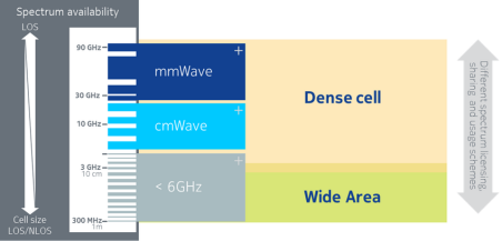
Figure 1 – frequency spectrum with sub-6 GHz and mmWave bands highlighted
1.2 Critical Role of Stack-Up Design in 5G Performance
The PCB stack-up the carefully orchestrated arrangement of copper layers, dielectric materials, and core substrates serves as the foundation upon which all 5G signal integrity depends. At mmWave frequencies, electromagnetic energy behaves according to principles that seem almost counterintuitive to designers accustomed to lower-frequency applications. Signal wavelengths shrink to millimeter scale, making
features like via stubs and trace discontinuities that were insignificant at 1 GHz become major sources of signal reflection and loss at 28 GHz.
A properly designed 5G PCB stack-up must simultaneously address multiple competing requirements: controlled impedance to prevent signal reflections, low insertion loss to preserve signal strength, effective electromagnetic interference (EMI) shielding to prevent crosstalk between circuits, and robust thermal management to dissipate heat from power-hungry RF amplifiers. The stack-up configuration directly impacts each of these parameters, making it the single most critical decision in the entire 5G PCB design process.
2. Understanding 5G PCB Requirements
2.1 5G Frequency Spectrum and Signal Characteristics
Sub-6 GHz Bands: Foundation for Widespread Coverage
The sub-6 GHz spectrum, encompassing frequencies from 600 MHz to 6 GHz, represents 5G’s coverage backbone. These lower frequencies provide the propagation characteristics necessary for wide-area network deployment, offering superior building penetration and longer range compared to mmWave. From a PCB design perspective, sub-6 GHz signals present moderate challenges more demanding than 4G LTE but less extreme than mmWave applications.
mmWave Bands (24-77 GHz): Extreme Precision Requirements Millimeter wave 5G, operating primarily in the 24 GHz, 28 GHz, 39 GHz, and 77 GHz bands, pushes PCB technology to its limits. At 28 GHz, the wavelength in a typical Rogers RO4350B laminate (Dk = 3.48) measures just 5.7 mm. This means a quarter wavelength stub a critical resonant length spans only 1.4 mm. Traditional plated through-hole vias, which routinely leave 2-3 mm stubs, become significant parasitic resonators that can completely destroy signal integrity.
Figure 2 – Detailed wavelength comparison showing physical dimensions
2.2 Key Electrical Parameters for 5G Stack-Ups
Several electrical parameters govern 5G PCB performance, each requiring careful consideration during stack-up design. The dielectric constant (Dk or εr) determines signal propagation velocity and controlled impedance values. For 5G applications, Dk stability across both frequency and temperature is paramount. A material whose Dk varies by 5% over temperature will cause impedance variations that generate reflections and degrade signal integrity in precision RF circuits.
The dissipation factor (Df), also called loss tangent (tan δ), quantifies dielectric losses. Standard FR-4 exhibits Df values of 0.015-0.020 at 10 GHz, while high-performance materials like Rogers RO3003 achieve 0.0010 at the same frequency a 15-20x improvement.
Impedance control tolerances tighten dramatically for 5G applications. While ±10% impedance tolerance might suffice for many applications, 5G RF circuits typically require ±5% or tighter control.
| Material | Dielectric Constant (Dk) | Dissipation Factor (Df) | Best Application |
| FR-4 Standard | 4.2-4.5 @ 1GHz | 0.015-0.020 | Digital, sub-6 GHz non-critical |
| Rogers RO4350B | 3.48 @ 10GHz | 0.0037 | Sub-6 GHz RF, cost-effective mmWave |
| Rogers RO3003 | 3.00 @ 10GHz | 0.0010 | High-performance mmWave, base stations |
| RT/duroid 5880 | 2.20 @ 10GHz | 0.0009 | Ultra-low loss >20 GHz, phased arrays |
Table 1: High-frequency laminate material comparison for 5G PCB applications
2.3 Physical and Thermal Requirements
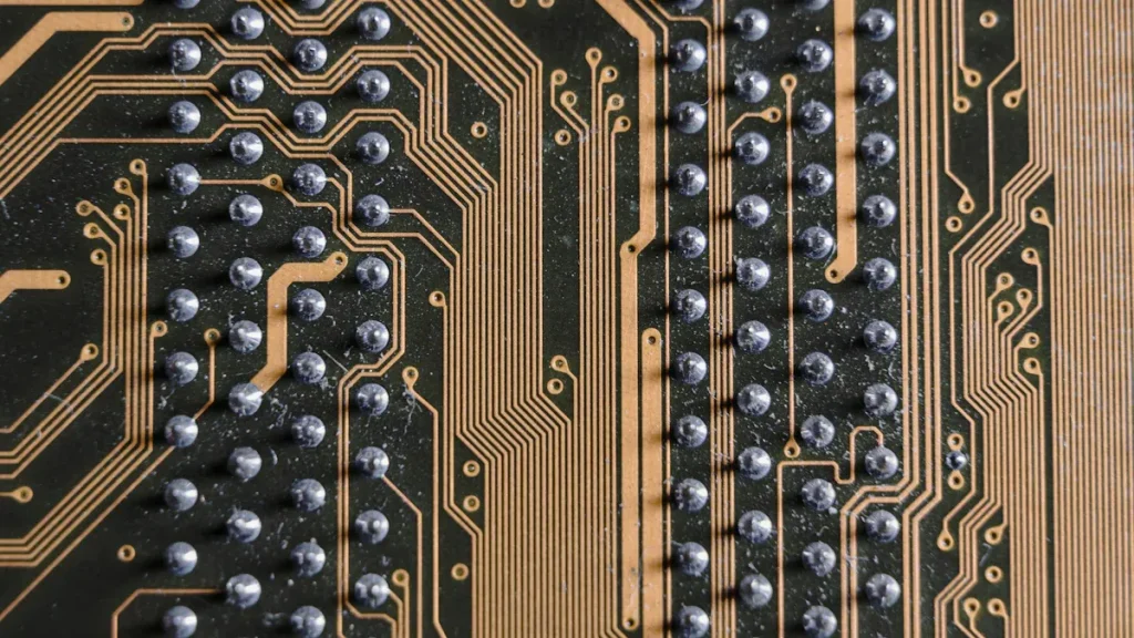
5G PCBs typically require 10-16 copper layers to accommodate the dense routing requirements of modern RF transceivers, baseband processors, power management circuits, and associated digital interfaces. High-density interconnect (HDI) technology featuring microvias as small as 0.1 mm diameter, blind and buried vias, and any-layer routing becomes essential for achieving the component density that 5G system integration demands while maintaining controlled impedance signal paths.
Thermal management presents significant challenges in 5G designs. Power amplifiers in base station applications can dissipate 50-100 watts, generating localized hotspots that reach 85-100°C during operation. The PCB substrate must possess sufficient thermal conductivity (≥1.5 W/m·K) to spread this heat across the board area and transfer it to heat sinks or thermal management systems. High-temperature resistance, measured as Relative Thermal Index (RTI) of ≥150°C, ensures material stability under sustained operating conditions.
Manufacturing tolerances tighten considerably for 5G PCBs. Registration accuracy the alignment precision between copper layers must reach ±75 μm (±3 mils) or better for mmWave applications, compared to ±150 μm for conventional designs.
3. Material Selection for 5G Stack-Ups
3.1 High-Frequency Laminate Materials
Rogers Materials: Industry Standard for RF Performance
Rogers Corporation’s high-frequency laminates have become the de facto standard for 5G PCB applications, offering carefully engineered dielectric properties that remain stable across wide frequency and temperature ranges. The RO4000 series, particularly RO4350B, strikes an excellent balance between RF performance and manufacturability. With a dielectric constant of 3.48 ±0.05 and dissipation factor of 0.0037 at 10 GHz, RO4350B provides predictable impedance control while utilizing standard FR-4 processing techniques no special via treatments or modified drilling parameters required.
For applications demanding even lower loss, the RO3000 series delivers exceptional performance. RO3003, with its ceramic-filled PTFE construction, achieves Df of 0.0010 and Dk of 3.00 properties that remain remarkably consistent from 10 MHz to 40 GHz. This material excels in base station power amplifier designs and other applications where every tenth of a dB of insertion loss impacts system performance. The trade-off comes in higher material costs (typically 3-5x RO4350B) and more demanding fabrication requirements.
Figure 3 – Cross-sectional view of Rogers RO4350B laminate construction showing copper foil, resin system, and glass reinforcement
3.2 FR-4 in 5G Applications: Understanding the Limitations
Standard FR-4 remains viable for specific portions of 5G designs, particularly digital signal processing sections, power distribution networks, and sub-6 GHz applications where RF performance requirements are less stringent. Modern high-quality FR-4 from manufacturers like Shengyi, Panasonic, and ITEQ can achieve Df values of 0.012-0.015 at 5 GHz when using appropriate resin systems and glass reinforcements
acceptable for many sub-6 GHz signal paths.
However, FR-4’s limitations become pronounced at higher frequencies. The material’s Dk typically varies by ±10% across the operating temperature range (-40°C to +85°C), compared to ±2% for high-frequency laminates. This variation translates into impedance fluctuations that can cause reflection-induced bit errors in high-speed digital interfaces and degrade RF system performance. Additionally, FR-4’s glass reinforcement creates localized variations in effective Dk the ‘fiber weave effect’ which becomes problematic for traces running at oblique angles to the glass fiber pattern.
3.3 Hybrid Stack-Up Strategies: Optimizing Performance and Cost
Hybrid stack-ups combining high-frequency laminates with FR-4 offer an excellent approach to balancing performance and cost in complex 5G designs. The core strategy places expensive low-loss materials only where RF signals travel, while using economical FR-4 for inner layers carrying digital signals, power distribution, and mechanical support. A typical hybrid stack-up might use Rogers RO4350B for the outer two layers (L1 and L12 in a 12-layer design) where RF microstrip transmission lines reside, with FR-4 cores comprising the inner layers.

Figure 4 – Cross-sectional diagram of a 12-layer hybrid stack-up showing Rogers RO4350B outer layers for RF signals
4. Layer Configuration Strategies for 5G
4.1 Fundamental Stack-Up Principles
Before diving into specific layer configurations, several fundamental principles govern all professional 5G PCB stack-up designs. Symmetry ranks as the most critical manufacturing consideration: the stack-up must be balanced around the board’s centerline to prevent warpage during lamination and thermal cycling. This means matching copper weights, core thicknesses, and prepreg counts on opposite sides of the center plane. A board that’s copper-heavy on one side will bow like a potato chip after reflow soldering an unacceptable outcome for precision RF assemblies.
Reference plane adjacency is equally important: every signal layer should have an uninterrupted ground or power plane immediately adjacent to it. This provides the low inductance return path that high-frequency signals require while simultaneously shielding the signal layer from interference.
Layer pairing involves grouping signal layers by function and electrical requirements. High-speed differential pairs should route on the same layer, with length matching achieved through serpentine routing rather than splitting pairs across layers. RF signal layers typically occupy outer layers where they can be implemented as microstrip transmission lines, providing easy access for tuning and debug.
4.2 8-Layer Stack-Up: Entry Point for 5G Designs
An 8-layer stack-up represents the minimum practical layer count for basic 5G applications such as IoT devices, small cell radios, or simple sub-6 GHz RF modules. While limited compared to higher layer counts, a well-designed 8-layer structure can effectively support moderately complex designs with careful routing discipline and component placement.
Recommended 8-Layer Configuration:
∙ Layer 1: RF Signal & Critical High-Speed (microstrip, 50Ω)
∙ Layer 2: Ground Plane (primary RF return path)
∙ Layer 3: High-Speed Digital Signals (stripline, 50Ω or 100Ω differential) ∙ Layer 4: Power Plane (+3.3V, +1.8V split)
∙ Layer 5: Power Plane (mirrored: +3.3V, +1.8V split)
∙ Layer 6: High-Speed Digital Signals (stripline, orthogonal to L3)
∙ Layer 7: Ground Plane (secondary return path)
∙ Layer 8: RF Signal & Critical High-Speed (microstrip, 50Ω)
This configuration provides symmetry (L1-L2-L3-L4 mirrors L8-L7-L6-L5), ensures every signal layer has an adjacent reference plane, and places power planes in the center where their capacitance best serves decoupling. Typical dielectric thicknesses might be: L1-L2 = 6 mils (RO4350B for RF), L2-L3 = 8 mils (core), L3-L4 = 14 mils (prepreg), L4-L5 = 20 mils (core), mirrored symmetrically to L8.
4.3 12-Layer Stack-Up: Advanced 5G Applications
For sophisticated 5G systems base station modules, massive MIMO antenna arrays, or high-end smartphones a 12-layer stack-up provides the routing density and signal integrity performance required for optimal results. The additional layers enable
complete isolation of RF, digital, and power sections while providing multiple ground planes for superior shielding.
Optimized 12-Layer Configuration for mmWave:
∙ Layer 1: RF Signal Layer A (mmWave antenna feeds, microstrip 50Ω) ∙ Layer 2: Ground Plane A (primary RF return, 1 oz Cu)
∙ Layer 3: RF Signal Layer B (secondary RF paths, stripline 50Ω)
∙ Layer 4: Ground Plane B (RF isolation and return, 1 oz Cu)
∙ Layer 5: Power Plane A (RF power: +5V PA supply, 2 oz Cu)
∙ Layer 6: High-Speed Digital (SerDes, DDR, PCIe stripline)
∙ Layer 7: High-Speed Digital (orthogonal routing to L6)
∙ Layer 8: Power Plane B (Digital power: +3.3V, +1.8V, +1.2V splits, 2 oz Cu) ∙ Layer 9: Ground Plane C (digital return and shielding, 1 oz Cu)
∙ Layer 10: Low-Speed Signals & Routing (control, I2C, SPI)
∙ Layer 11: Ground Plane D (final shielding layer, 1 oz Cu)
∙ Layer 12: RF Signal Layer C (secondary RF, component placement, microstrip 50Ω) This S-G-S-G-P-S-S-P-G-S-G-S configuration provides exceptional performance: four separate ground planes create multiple shielding barriers, RF layers are completely isolated from digital switching noise, and stripline RF routing on L3 offers excellent shielding for sensitive paths. The stack-up maintains symmetry about the L6-L7 center plane.
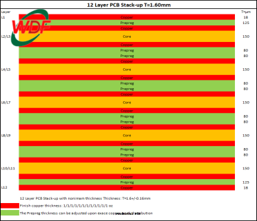
Figure 5 – Detailed cross-section of a 12-layer 5G PCB stack-up showing layer thicknesses, copper weights, and signal/plane
5. Grounding Techniques for 5G PCBs
5.1 Grounding Fundamentals for High-Frequency Design
At high frequencies, ground is not simply a zero-voltage reference point but rather a complex electromagnetic structure whose behavior dominates signal integrity performance. The fundamental principle: high-frequency return currents flow directly beneath their associated signal traces, following the path of minimum impedance. This path depends not on DC resistance but on inductance return currents naturally concentrate in the region of maximum magnetic field coupling with the signal conductor.
The skin effect at mmWave frequencies means return currents flow only in the top few hundred nanometers of the ground plane’s surface. This makes surface finish and oxidation potential surprisingly important tarnished copper exhibits higher RF resistance than bright copper. For this reason, many designers specify ENIG (Electroless Nickel Immersion Gold) surface finishes on ground planes in critical RF areas, despite the slight additional inductance the nickel layer introduces.
5.2 Solid Ground Plane Implementation
A continuous, unbroken ground plane represents the single most important feature of any high-frequency PCB stack-up. Think of the ground plane as providing a perfectly smooth lake surface for return currents to flow any obstruction (void, slot, cutout) creates turbulence that radiates energy and reflects signals. For 5G applications, ground plane integrity is non-negotiable: every ground plane should extend from edge to edge of the board with minimal interruptions.
When ground plane splits become unavoidable perhaps to separate analog and digital sections, or to create thermal relief around mounting holes use stitching capacitors to bridge the gap. Place 0.1 μF or smaller capacitors at 1-2 inch intervals along the split, providing an AC short at RF frequencies while maintaining DC isolation. Never route high-speed or RF signals across ground plane splits; if a trace must cross a split, route it perpendicular to minimize the loop area and add a ground via immediately adjacent to the crossing point.
5.3 Via Stitching and Ground Fencing Techniques
Via stitching the strategic placement of grounding vias to connect ground planes between layers ranks among the most critical yet often overlooked aspects of 5G PCB design. At mmWave frequencies, the inductance of even a short ground connection becomes significant. A single 10 mil diameter via through a 62 mil thick board exhibits roughly 0.7 nH of inductance seemingly negligible, but at 28 GHz this represents an impedance of approximately 123 ohms, sufficient to severely degrade high-frequency ground connections.
The solution lies in parallel via arrays. Using four vias in parallel reduces the effective inductance by roughly 4x (accounting for mutual inductance effects), bringing the connection impedance to more acceptable levels. For critical RF components, place 3-4 ground vias immediately adjacent to each ground pin, connecting to the nearest
solid ground plane. Space these vias as close to the component as possible inductance increases with via length, making short paths essential.
Figure 6 – Top view of PCB layout showing via stitching pattern around
6. Impedance Control in 5G Stack-Ups
6.1 Controlled Impedance Fundamentals
Controlled impedance represents the foundation of high-speed and RF signal integrity. When a signal’s source, transmission path, and termination all present the same characteristic impedance, energy transfers completely from source to load with no reflections. Impedance mismatches cause portions of the signal to reflect back toward the source, creating standing waves, ringing, and intersymbol interference that corrupt digital signals and degrade RF system performance.
For 5G applications, 50-ohm single-ended impedance has become the universal standard for RF and microwave circuits. This value emerged from optimization between power handling capability and loss in coaxial cables, and the entire RF ecosystem connectors, test equipment, components assumes 50-ohm systems. High
speed digital interfaces typically use either 50-ohm single-ended (for single-ended signals like clocks) or 100-ohm differential impedance (for differential pairs like MIPI, PCIe, and USB).
6.2 Microstrip Configuration for RF Signals
Microstrip a signal trace on the board’s outer layer with a ground plane on the adjacent inner layer represents the most common transmission line configuration for RF circuits.
The characteristic impedance of a microstrip depends on trace width (W), height above the ground plane (H), copper thickness (T), and the dielectric constant of the substrate material (εr). For a first-order approximation, wider traces and thicker dielectrics increase impedance, while higher dielectric constants decrease impedance.
Example microstrip calculation: achieving 50Ω on 5-mil thick Rogers RO4350B (εr = 3.48) with 1 oz copper requires approximately 11 mil trace width. The same impedance on 4-mil dielectric requires 8.5 mil width demonstrating the sensitivity to dielectric thickness.
Figure 7 – Cross-sectional diagram of microstrip transmission line geometry
6.4 Differential Pair Impedance for High-Speed Interfaces
Differential signaling transmitting data as the voltage difference between two complementary signals dominates modern high-speed digital interfaces due to superior noise immunity and reduced EMI. The differential impedance (Zdiff) depends on both the single-ended impedance of each trace (Z0) and the coupling between the traces. For loosely coupled traces, Zdiff ≈ 2 × Z0. As traces move closer together, coupling increases, reducing differential impedance below this 2:1 ratio.
For 100-ohm differential impedance (the standard for most high-speed digital interfaces), typical designs use 50-ohm single-ended traces with coupling that reduces the differential impedance to 100 ohms. In microstrip with edge-coupled traces, achieving 100-ohm differential typically requires trace spacing of 1.5-2× the trace width. Tighter spacing increases coupling and further reduces differential impedance; wider spacing decreases coupling and raises differential impedance.
| Layer | Function | Type | Cu Weight | Thickness | Material |
| L1 | RF Signal | Microstrip 50Ω | 0.5 oz | – | RO4350B |
| L2 | Ground | Plane | 1 oz | 5 mil | Core |
| L3 | RF Signal | Stripline 50Ω | 0.5 oz | 6 mil | Prepreg |
| L4 | Ground | Plane | 1 oz | 8 mil | Core |
| … | Symmetric | Mirror | … | … | … |
Table 2: Example 12-layer 5G stack-up configuration (partial) showing top layers
7. Signal Integrity Considerations
Signal integrity in 5G PCBs encompasses multiple interrelated phenomena that can degrade system performance if not properly managed. Understanding the mechanisms of signal degradation and the stack-up design techniques that mitigate them separates functional designs from optimal ones.
7.1 High-Frequency Loss Mechanisms
Signal loss increases dramatically with frequency due to multiple physical effects. Dielectric loss arises from molecular polarization in the substrate material as the electric field oscillates at RF frequencies, dipoles in the material attempt to align with the field, dissipating energy as heat. This loss directly correlates with the dissipation factor: doubling Df approximately doubles loss. At 28 GHz in standard FR-4 (Df ≈ 0.020), dielectric losses can exceed 1.5 dB per inch, while Rogers RO3003 (Df ≈ 0.001) achieves losses below 0.3 dB per inch under identical conditions. Conductor loss increases with the square root of frequency due to skin effect high-frequency currents concentrate near conductor surfaces, increasing effective resistance.
7.2 Via Design for mmWave Applications
Via stubs the unused portion of a through-hole via that extends past the layer where the signal exits create resonant structures that reflect signals at specific frequencies. The stub acts as a short-circuited transmission line whose quarter-wavelength resonance causes maximum reflection. At 28 GHz with a 50 mil board thickness, even a 15 mil stub can create problematic resonances. Solutions include back-drilling to remove stubs or using blind/buried vias that terminate exactly at the signal layer.
Figure 9 – Back Drilled PCB via
Conclusion
Successful 5G PCB stack-up design needs expertise of multiple disciplines i.e material science, electromagnetic theory, manufacturing processes, and thermal management. The guidelines presented in this article from material selection through grounding strategies to impedance control provide a comprehensive framework for creating high
performance 5G designs.
Major Results include:
1. Material selection drives performance and cost use high-frequency laminates where needed, FR-4 elsewhere.
2. Symmetrical stack-ups with proper reference planes are non-negotiable. 3. Ground plane integrity and via stitching determine signal integrity at mmWave.
4. Impedance control requires precise dielectric thickness control and field solver verification.
5. Early collaboration with your PCB manufacturer prevents costly respins.
As 5G technology continues evolving toward higher frequencies and greater complexity, the steps and methods outlined here will remain fundamental. Whether you’re designing your first 5G product or optimizing an existing platform, investing time in stack-up optimization pays dividends in system performance, manufacturing yield, and time-to-market.