Knowing the words used in PCB design is important. It helps you talk clearly with engineers and manufacturers. This shared understanding prevents errors and makes teamwork easier. PCB terms also help you understand tough ideas faster. This makes your work quicker and better. Whether you make a simple circuit or a complex board, learning these words is key.
Learning these terms is the first step to feeling confident in PCB design.
Key Takeaways
Knowing PCB terms helps you talk clearly with engineers and makers.
The base, copper layer, solder mask, and silkscreen are main parts of a PCB that make it strong and work well.
Picking the right parts like resistors, capacitors, and chips is key for circuits to work their best.
Different PCBs, like single-sided, double-sided, and multilayer, fit different projects and needs.
Drawing traces and pads the right way keeps signals clear and stops overheating.
A Bill of Materials (BOM) lists all the parts needed to build a PCB, helping avoid mistakes and save money.
Testing methods like checking connections and functions make sure PCBs work before use.
Good heat control, like using heat sinks and thermal vias, stops overheating and keeps things working well.
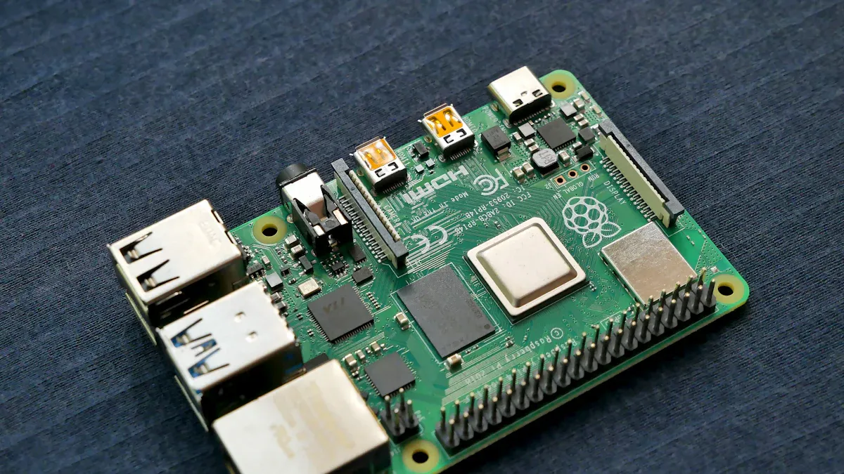
PCB Structure and Components
Layers of a Printed Circuit Board
Substrate
The substrate is the base of a PCB. It holds everything together and keeps the board strong. Most PCBs use FR-4, a material made of fiberglass and epoxy. This material is tough and affordable, making it great for many uses.
Copper Layer
The copper layer helps electricity flow through the PCB. Thin copper sheets are attached to the substrate. These sheets form paths and spots to connect parts. A good copper layer improves signals and reduces electrical noise.
Performance Improvement | Description |
|---|---|
Better Noise Control | Cuts down noise and improves signals. |
Smaller Designs | Fits more parts in less space. |
Easier Wiring | Keeps paths clear in fast circuits. |
Heat Control | Helps cool the board for better performance. |
Solder Mask
The solder mask keeps the copper safe from rust and stops solder from spreading during assembly. It’s the colored layer you see on PCBs, often green. This layer protects the paths and keeps them working well.
Silkscreen
The silkscreen adds labels and markings to the PCB. It shows where parts go and helps with testing and fixing. Clear labels make building and repairing the board easier.
Key Components in PCB Design
Resistors
Resistors slow down the flow of electricity. They keep voltage steady and protect delicate parts.
Capacitors
Capacitors store and release energy. They help keep voltage stable and reduce noise for smooth operation.
Inductors
Inductors store energy using magnets. They control current and reduce noise in power supplies and filters.
Integrated Circuits (ICs)
ICs are tiny circuits that do specific jobs. They can be simple or very advanced, like microprocessors. Picking the right IC makes your PCB work better.
Best Practice | Description |
|---|---|
Part Placement | Keeps parts working without problems. |
Voltage Levels | Matches correct voltage for strong connections. |
Power and Ground | Helps heat flow and makes the board last longer. |
Vias Placement | Keeps signals strong between layers. |
Shielding | Protects sensitive parts for better performance. |
Connectors
Connectors join the PCB to other devices or boards. They allow smooth communication and power sharing between systems.
Make sure the microcontroller has the right speed and ports.
Look into new tech like wireless modules for better designs.
Check if all parts work well together for smooth operation.
Types of PCBs
Single-Sided PCB
Single-sided PCBs have parts and paths on one side only. They are cheap and good for simple projects.
Double-Sided PCB
Double-sided PCBs have paths on both sides. They give more options for wiring and work well for medium-level designs.
Multilayer PCB
Multilayer PCBs have many layers of base and copper. They handle complex circuits and save space. These boards are popular because they work well and are flexible.
Multilayer PCBs are great for their small size and strong performance.
They handle complicated circuits needed for advanced systems.
They manage heat better, making them reliable and cost-effective.
Rigid vs. Flexible PCBs
Rigid PCBs are hard and keep their shape. Flexible PCBs can bend and fit into unique designs. Flexible boards are perfect for wearable gadgets and small electronics.
Design and Layout Words in PCB Design
Important Design Parts
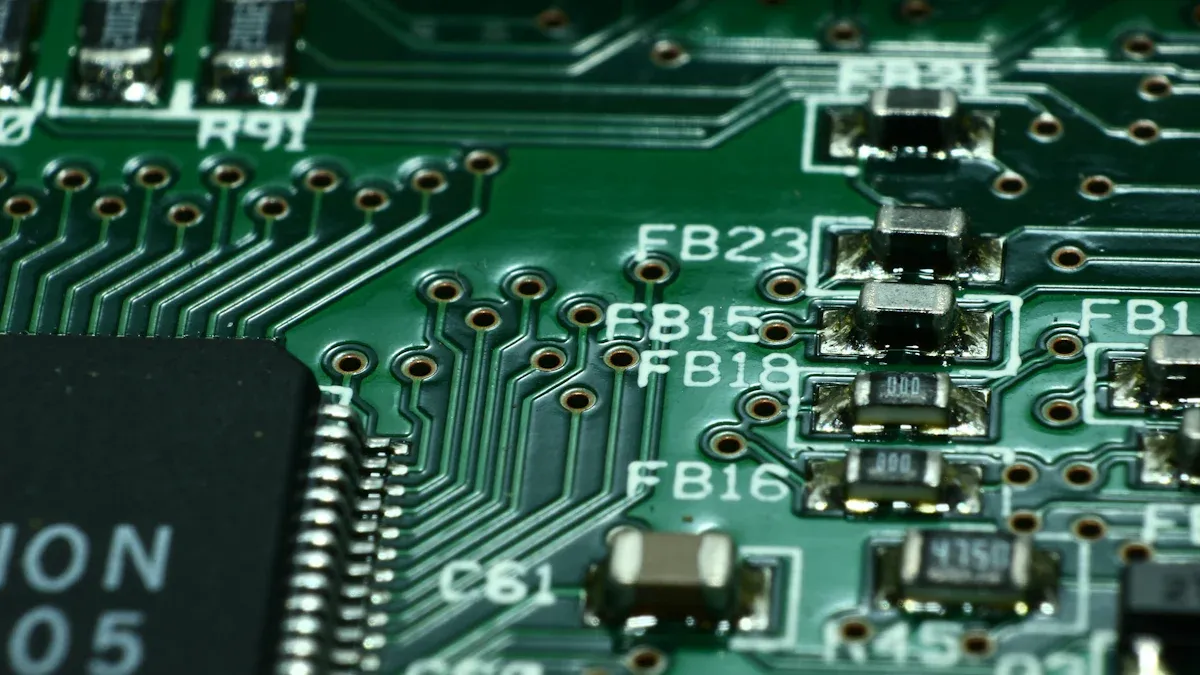
Traces
Traces are thin copper lines on a PCB. They carry signals between parts, like roads connecting cities. Traces must be designed to handle current and avoid problems. Wider traces carry more current, while thinner ones save space. Good trace design keeps signals smooth and prevents overheating.
Pads
Pads are small copper spots where parts are soldered. They connect parts to the board. There are two main pad types: through-hole and surface-mount. Through-hole pads have holes for part leads, while surface-mount pads are flat for tiny parts. Pick the right pad based on your parts and assembly method.
Vias
Vias are tiny copper-filled holes linking PCB layers. They let signals move between layers, which is key for complex boards. There are three via types: through-hole, blind, and buried. Through-hole vias go through the whole board. Blind and buried vias link specific layers. Placing vias well improves signals and reduces noise.
Ground Plane
The ground plane is a big copper area on a PCB. It gives a common path for currents to return. It lowers noise and improves signal quality. A good ground plane also helps cool the board. Pair it with a power plane for a stable setup.
PCB Design Software and Files
CAD Tools
CAD tools help you design PCB layouts. They let you place parts and draw traces accurately. Popular tools include Altium Designer, KiCad, and Eagle. CAD software ensures your design follows rules and avoids mistakes.
Gerber Files
Gerber files are used to make PCBs. They include details like copper layers, solder mask, and silkscreen. After designing, export Gerber files to share with manufacturers. Accurate Gerber files make production smooth.
Design Rules and Limits
Clearance
Clearance is the smallest space between PCB parts. Keeping proper clearance stops short circuits and ensures the board works. CAD tools check if your design meets clearance rules.
Checking design rules is a key step in PCB design. It ensures the board will work, can be made, and is reliable.
Impedance Control
Impedance control is vital for fast PCB designs. It keeps signals clear as they travel. You control impedance by adjusting trace width, spacing, and materials. This is crucial for communication and data boards.
Signal Integrity
Signal integrity means keeping signals clear on a PCB. Bad signal integrity causes data loss and errors. To keep signals strong, reduce noise, avoid sharp trace angles, and use good grounding.
Good PCB design data avoids problems during building and testing.
Bad data causes costly fixes, delays, and extra work.
Set standards, check data, use automation, and review carefully for success.
Manufacturing and Assembly Terms in PCB Design
PCB Fabrication Processes
Etching
Etching removes extra copper to form traces and pads. A chemical solution dissolves the unwanted copper, leaving the circuit design. This process ensures the PCB layout is accurate, even for complex boards. Good etching reduces mistakes and makes the board more reliable.
Drilling
Drilling makes holes for vias and through-hole parts. Machines drill these holes with great precision for proper alignment. The size and location of the holes are important for strong signals and stability. Advanced drilling methods make production faster and reduce mistakes.
Plating
Plating adds a thin metal layer to holes and traces. This layer improves conductivity and strengthens connections. Materials like gold or tin are often used to prevent rust. High-quality plating helps the PCB work well in different conditions.
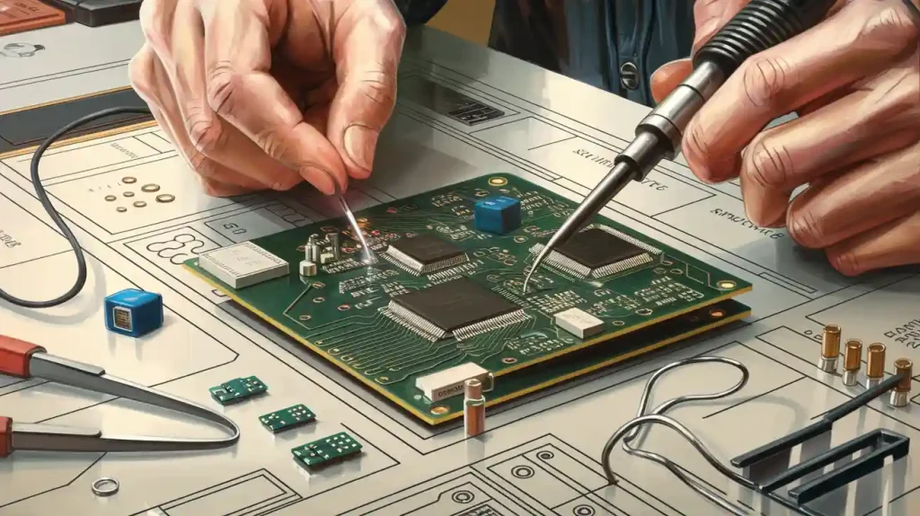
Assembly Techniques
Surface Mount Technology (SMT)
Surface mount technology places parts directly on the PCB surface. This method is quicker and more efficient than older techniques. SMT allows for smaller, compact designs, perfect for modern devices.
Efficiency Metrics:
Line Efficiency: Measures how much time is used for placing parts.
Output per Employee: Each worker assembles about 4.6 million parts yearly.
Components Assembled per Machine: Each machine places 2,340 parts every hour.
These numbers show how SMT speeds up production while keeping quality high.
Through-Hole Technology (THT)
Through-hole technology inserts part leads into drilled holes and solders them. THT creates strong bonds, making it good for parts under physical stress. Though slower than SMT, THT is still used for durable items like power supplies.
Soldering Methods
Reflow Soldering
Reflow soldering uses heat to melt solder paste and attach parts to the PCB. The board goes into a reflow oven, where controlled heat ensures proper soldering. This method works well for SMT parts and large-scale production.
Wave Soldering
Wave soldering passes the PCB over molten solder to attach parts. This method is great for THT parts, ensuring strong and even connections.
Quality Outcomes:
Different solder types, like SAC+SAC and LT+LT, perform similarly in tests.
Higher heat improves joint strength by forming thicker layers.
Best results happen within 3-4 seconds of solder contact.
Both methods help create strong connections and reduce assembly errors.
Bill of Materials (BOM)
What is a BOM and Why It Matters
The Bill of Materials (BOM) is a list of all parts needed to make a printed circuit board. It works like a guide for building the board, making sure no part is forgotten. A BOM usually includes details like part numbers, amounts, descriptions, and where to buy them. This list helps you stay organized and ensures nothing important is left out during production.
Think of the BOM as a shopping list for your PCB. It tells the manufacturer exactly what to use to build the board. Without a clear BOM, mistakes can happen, like using the wrong part or running out of supplies. A good BOM saves time and avoids errors, making production easier.
Tip: Always check your BOM carefully before sending it to the manufacturer. This step avoids mistakes and keeps things on schedule.
A BOM also helps you control costs. By listing all parts, you can compare prices from different suppliers and pick the cheapest options. This is very helpful for big projects, where saving even a little on each part can save a lot of money.
Besides saving money, the BOM helps you work better with the manufacturer. It gives a clear list to talk about changes or fix problems. For example, if a special solder is needed, the BOM makes sure this is not missed.
Key Benefits of a BOM | Description |
|---|---|
Fewer Errors | Stops missing or wrong parts during assembly. |
Cost Savings | Helps find cheaper parts to save money. |
Faster Production | Gives clear steps for quick manufacturing. |
Better Communication | Makes sure everyone knows what’s needed. |
Making a BOM might take time, but it’s very important in PCB design. It keeps your project on track and ensures the final board works as planned. Whether your design is simple or complex, a detailed BOM is the key to success.
Electrical and Testing Concepts in PCB Design
Key Electrical Properties
Capacitance
Capacitance shows how well a part can store energy. It helps keep voltage steady and reduces noise in circuits. Adding capacitors in parallel increases capacitance, while in series, it decreases. This is important for smooth power and stable signals.
Key Formula:
The current in a capacitor depends on voltage change speed:I_cap = C * (dV/dt)
Inductance
Inductance is how a part stores energy in a magnetic field. Inductors block sudden current changes, helping in power supplies and filters. They lower noise and keep current steady. Placing inductors correctly improves performance and reduces interference.
Resistance
Resistance shows how much a part slows down current flow. Higher resistance means less current for the same voltage, protecting delicate parts. Choosing the right resistor values ensures safe current levels and prevents overheating.
Key Property | Effect on Circuit Performance |
|---|---|
Capacitance | Goes up with parallel, down with series placement. |
Resistance | Controls current; higher resistance lowers current flow. |
Dissipation Factor | Shows efficiency in AC; lower is better. |
Testing Techniques
Continuity Testing
Continuity testing checks if paths on the PCB are connected. It ensures traces, pads, and vias work properly. This test finds broken connections early and avoids bigger problems later.
Functional Testing
Functional testing checks if the PCB works as it should. It tests the board under real conditions to ensure all parts work together. This step is key to making sure the board performs well.
In-Circuit Testing (ICT)
In-circuit testing looks at each part on the PCB. It finds problems like bad soldering, shorts, or faulty parts. ICT gives detailed feedback, making it great for quality checks.
Testing Technique | Advantages | Limitations |
|---|---|---|
Visual Inspection | Quick and cheap for basic checks | Misses hidden problems |
Electrical Testing | Finds functional issues well | Needs special setups |
X-ray Inspection | Spots hidden defects without taking apart the board | Costs more |
Functional Testing | Tests full performance in real use | Takes more time |
Signal and Power Integrity
Crosstalk
Crosstalk happens when signals in nearby traces affect each other. This is worse in fast PCBs. To avoid it, keep traces apart and use a solid ground plane.
Electromagnetic Interference (EMI)
EMI is unwanted signals that mess up circuits. Bad grounding and close traces make EMI worse. Reduce EMI by routing traces carefully and shielding sensitive parts.
Power Distribution Network (PDN)
The PDN delivers stable power across the PCB. A good PDN lowers voltage drops and noise, making the board reliable. Use decoupling capacitors and a strong ground plane to improve it.
Factors Affecting Signal Integrity:
Fast signals increase crosstalk risk.
Poor grounding worsens EMI problems.
Uneven signal delays cause errors.
Tip: Focus on signal and power integrity early to avoid costly fixes later.
Advanced PCB Terminology
High-Speed PCB Design
Differential Pairs
Differential pairs are two traces carrying opposite signals. These traces help reduce noise and keep signals clear. Keeping them close together cancels out outside interference. This method is used in systems like USB and HDMI to keep signals strong.
To make differential pairs work well, keep their lengths the same. If one trace is longer, it can cause delays and errors. Also, keep the spacing between the traces even. Using controlled impedance traces helps avoid signal problems and keeps signals smooth.
Controlled Impedance
Controlled impedance makes sure signals move without distortion. It is very important for fast PCB designs. You control impedance by adjusting trace width, spacing, and materials between layers.
For example, placing a ground plane near fast signal layers blocks interference. Shorter traces and careful routing also reduce unwanted effects. These steps improve signal quality and make the board reliable for devices like smartphones and IoT gadgets.
Thermal Management in PCB Design
Heat Sinks
Heat sinks are metal parts that pull heat away from components. They stop parts from overheating, which can damage the board. Attaching a heat sink helps keep parts cool and safe.
For better cooling, use heat sinks with thermal pads or vias. This setup spreads heat evenly and improves cooling. Good thermal management keeps your PCB working well and lasting longer.
Thermal Vias
Thermal vias are small copper-filled holes that move heat between layers. They are useful for parts that get very hot. By connecting these parts to larger copper areas or heat sinks, thermal vias spread heat better.
Placing thermal vias in the right spots improves cooling a lot. Bad heat management can cause parts to fail early. Using thermal vias keeps your PCB reliable, even in tough conditions.
Design for Manufacturability (DFM)
Panelization
Panelization arranges many PCBs on one panel for easier production. This saves money and speeds up assembly. Designing with panelization reduces waste and simplifies manufacturing.
It also helps during soldering and testing. For example, breakaway tabs make it easy to separate boards after production. This method makes your design cheaper and simpler to produce.
Tolerances
Tolerances are small size differences allowed during manufacturing. Tight tolerances make parts more precise but cost more. Balancing tolerances keeps designs affordable and easy to make.
DFM checks find problems before production starts. For instance, keeping enough space between copper traces avoids short circuits. Fixing these issues early reduces mistakes and saves money. It also makes manufacturing smoother and faster.
Tip: Work with your manufacturer to understand their limits. This ensures your design fits their production process.
Common Acronyms in PCB Design
Knowing acronyms in PCB design makes teamwork easier. These short forms save time and help everyone understand each other. Below are some common acronyms used in design, making, and testing.
Acronyms for Design
PCB (Printed Circuit Board)
PCB means printed circuit board, the base of electronics. It links and holds parts using copper paths. Knowing this helps you talk about designs with engineers. PCB footprints show where parts go for proper placement. Silkscreen labels on the board guide assembly and fixing.
Why design acronyms help:
PCB footprints ensure correct part placement.
Silkscreen labels make parts easy to find.
Clear labels prevent mistakes during assembly.
CAD (Computer-Aided Design)
CAD tools help create PCB layouts. These programs let you draw circuits, place parts, and connect paths. CAD software ensures your design follows rules and avoids mistakes. It also helps teams work together by turning symbols into footprints. This makes fixing problems faster and easier.
Benefits of CAD tools:
Clear schematics for easy understanding.
Better teamwork with shared designs.
Faster fixes with clear part locations.
Acronyms for Manufacturing
SMT (Surface Mount Technology)
SMT is a way to place parts directly on a PCB. This method allows smaller designs and quicker production. SMT machines can place many parts quickly, perfect for modern devices. Metrics like TEEP and OEE measure how well SMT works in factories.
Acronym | Meaning |
|---|---|
TEEP | Total Effective Equipment Performance shows equipment potential. |
OEE | Overall Equipment Effectiveness checks factory efficiency. |
BOM (Bill of Materials)
The BOM lists all parts needed to build a PCB. It includes details like part numbers and amounts. A clear BOM ensures no parts are missed. It also helps compare prices to save money on big projects. A detailed BOM avoids delays and helps manufacturers.
Acronyms for Testing
ICT (In-Circuit Testing)
ICT tests each part on a PCB to check if it works. It finds problems like bad soldering or broken parts. ICT gives detailed results, making it great for quality checks. Using ICT ensures the board works before moving forward.
EMI (Electromagnetic Interference)
EMI means unwanted signals that mess up circuits. Bad grounding or close traces can cause EMI. To reduce EMI, route traces carefully and shield sensitive parts. Fixing EMI early makes your PCB more reliable.
Tip: Learn these acronyms to work better and speed up your PCB projects.
Knowing PCB terms helps you design better and work well with others. It makes talking with engineers and manufacturers easier, avoiding mistakes and delays. For instance, in airplanes, advanced PCBs make systems more reliable. In medical tools, multi-layer PCBs help signals move faster.
Why it matters:
Spotting signal problems early makes fast designs work better.
Using automation tools saves time and improves layouts.
Learn more about IoT gadgets, smart sensors, and car electronics to grow your skills. Understanding PCB terms leads to creative designs and successful projects.
FAQ
What does a PCB do?
A PCB links and holds electronic parts together. It organizes circuits neatly, making gadgets like phones, computers, and appliances work properly.
Why is the solder mask useful?
The solder mask keeps copper safe from rust and stops solder from spreading. It helps the board work well and look neat.
How do you pick the right PCB?
Think about your project’s needs. Simple designs use single-sided PCBs, while complex or small projects need multilayer or flexible ones.
What are Gerber files for?
Gerber files have all the details manufacturers need to make your PCB. They include info about copper layers, solder masks, and silkscreen designs.
How can EMI be reduced in PCB design?
Keep traces short and spaced out. Use a solid ground plane and shield important parts. These steps lower interference and improve signals.
How are SMT and THT different?
SMT puts parts on the board’s surface for smaller designs. THT uses drilled holes for stronger connections in tough conditions.
Why is impedance control important?
Impedance control keeps signals clear, especially in fast designs. It helps devices like communication systems work better.
What is a Bill of Materials (BOM)?
A BOM lists all the parts needed to build a PCB. It includes part numbers, amounts, and details to ensure smooth assembly and cost savings.
Tip: Always check your BOM carefully to avoid mistakes or delays.