1. Introduction to PCB Holes
PCB, or printed circuit board, is a very important component or building block for circuit creation on which different circuit components are connected. But the most important factor for PCB board designing and handling all components on board different types of holes are made with the use of different techniques and processes. Each type of hole has its own process of manufacturing and working performance. The main function of holes is to make it easy for components to mount on the board, providing strong and reliable electrical connections and structural strength for the PCB board. In this tutorial, we will cover various types of PCB holes that are important for accurate PCB design and production according to project demands. So let’s get started!

2. Types of PCB Holes
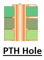
2.1 Plated Through-Holes (PTH)
Plated through holes, also known as electroless plating copper. These holes are drilled through the board and lined with the help of copper, which is a conductive material. Tin or gold is used for lining plating that helps to make the connection between PCB board layers.
The function of these holes is to make electrical connections between different PCB board layers or components connected to the board. These holes are also helpful in providing low resistance for component leads and copper wires and increasing PCB assembly mechanical stability.
Plated-through holes are also helpful for making strong connections between the double-sided board or multilayer board layers.
The main uses of PTHs are in resin copper plating, copper plating, or diamond copper plating.
2.2 Non-Plated Through-Holes (NPTH)
In this type of PCB hole, there is no copper used as plating onto hole walls; as a result, hole barrels do not have a conductive nature or electrical features. They are best to use where the board comes with copper tracks on a single side, but they are not a good option for multiple-layer boards since the use of these holes reduces the number of layers for the board.
However, the manufacturing of these holes is an easy and fast process and is used for tooling holes for fixing boards at the working point. They are also made for screws or bolt-like components, securing and used as a heat sink for heat dissipation.

2.3Half holes
The half holes in the PCB board, also called plate half holes or castellated holes, are partially drilled through holes made at the board edge, and these holes are milled halfway through. These holes are used for soldering another PCB on the main board. In simple words, make the connection between two separate boards, and they are the main part of high-density component connections. For the connection of Bluetooth on another board, plated-through holes are used.

2.3 Via Holes
The main purpose of via holes is to make strong electrical connections for different layers of PCB boards and also to be used for plated through-hole component connections, etc. The connection of different layers of multilayer boards through vias helps to ease signal flow between layers and connected components.
Blind Vias
The blind vias of the board are made from the top or lower layers to the inner layers and do not pass completely in the board like plated through vias. In this view, we cannot see the other side of the board.
These vias are made with the use of a mechanical drilling process, and sometimes lasers are used to drill blind vias. For drilling of these via types, make sure their accurate dimensions. Either it is a difficult process, but we can drill blind vias directly on the board.
The main use of blind vias is to make a connection to one external layer with a minimum of one inner layer. The aspect ratio for these vias is 1:1 or larger.
The blind vias are part of HDI PCB manufacturing, but make sure that the board that has blind vias is not always HDI PCB.

Buried vias
The buried vias are made between internal layers of the PCB board, and these are not seen from the external side of the board. The main purpose of these vias is to make connections between 2 or more inner layers. For every connection level, define holes as separate drill files.
The aspect ratio for buried vias is 1:12 or larger.
According to IPC standards, the recommended diameter for blind vias and buried vias is not larger than 6 mils.
Stacked Vias
Stack vias are blind vias or buried vias that are used for making connections between different board layers for more than three circuit layers. The stacked vias come with two or more vias configured on each other that traverse many layers of boards.
The main uses of stacked vias are in multilayer boards and also in HDI boards. The design of stacked vias is such that each vai in the stack is configured with one internal layer of the board.
The main feature of these vias is to provide continuous electrical connections in different layers. The projects where space is limited but complex design stacked vias are used.

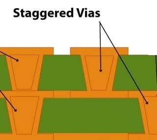
Staggered Vias
The staggered vias are made when different PCB board layer vias are connected but not overlapping. The staggered vias come with many vias in such connections that do not have a direct connection since drill axes are different.
The staggered vias make a zigzag pattern on the board when we view the board from any side. The main uses of staggered vias are in HDI boards and multilayer PCBs.
Skip Vias
This via passes many layers of the board but does not have any electrical connection with any layer. Skip vias can be overlapping vias, blind vias, or buried vias. These vias are important for the HDI board for making compact and complicated circuits. Skip vias make vertical electrical connections between board layers that make dense component packing and reduce signal path length.
Vias-in-Pad
Via in the pad is a less common type of PCB vias, and in this design, the via is made directly under the surface mount component pad rather than routing the trace about the pad. Via the connection of the component pad on the upper layers with the inner layer of the board.
The main features that help to use these vias are that they provide easy routing and control parasitic inductance. Its disadvantage is that at the time of reflow, soldering solder paste passes through vias and affects soldering on the PCB pad.
2.4 Mounting Holes
Mounting holes are made in the PCB to provide points for mounting the board with the chassis. These holes have larger sizes than other hole types of board and are normally made on board corners. For making a strong and stable connection between the board and mounting components, copper pads are applied around the mounting holes.
2.5 Countersink and Counterbore Holes
Counterbore holes are made for bolts or screws and come with flat-bottomed heads that have a larger size as compared to screw designs. These holes come with 2 diameter holes, a larger diameter at the upper part for handling the screw head and a small diameter for having a screw or bolt body.
Countersinks are used for applications where screws needed to have tapered heads. These holes are made at a conical angle that is according to the taper of the screw’s upper part of the head that helps the screw to sit flush on the board surface. For making countersinks, normally 82 or 90 degrees drill bits are used.
image Countersink and Counterbore Holes

2.6 Fiducial Holes (Alignment Holes)
Fiducial holes, called alignment holes, are small-sized and defined holes drilled on board that are used as reference points for automated manufacturing tools. Their main feature is to provide accurate alignment at times of different phases, such as component connection, stencil process, and testing, that make sure all components on boards are connected accurately for board assembly.
Image: Fiducial holes

2.7 Special PCB Hole Types
- Stamp Holes
Stamp holes, also called breakaway holes, are small-sized holes made in sequence or row with edges of every circuit board in the panel. These holes look like the edges of stamps, so they are known as stamp holes. The main use of these holes is for PCB depanelization. In the depanelizing process, a single board is separated from the larger panel. That process is used to increase production efficiency and reduce expenses.
3. PCB Hole Design Considerations
Many factors must be considered for PCB hole design that are listed here.
Hole Size & Aspect Ratio
The value of hole size is based on drilling techniques and the layer count of the board. The ratio of hole depth to hole diameter is called the aspect ratio.
| Drilling Technique | Min. Hole Diameter | Max. Aspect Ratio |
| Mechanical Drilling | 0.2 mm | 10:1 |
| Laser Drilling (Microvias) | 0.075 mm | 1:1 to 1.5:1 |
| Chemical Etching | ~50 µm | ~1:1 |
| EDM (Electrical Discharge) | 0.1 mm | 5:1 |
| Ultrasonic Drilling | 0.2 mm | 5:1 |
Drill Tolerance & Annular Ring Details
The annular ring is copper covering about the plated hole. If there is no proper width of the ring, it causes issues for board reliability.
| Hole Size (mm) | Drill Tolerance (± mm) | Min Annular Ring (mm) |
| ≤ 0.3 | ±0.025 | 0.1 |
| 0.3 – 0.6 | ±0.05 | 0.15 |
| > 0.6 | ±0.075 | 0.2 |
Plating Thickness for PTH & Vias
The plating thickness according to design requirements provides good mechanical strength for the board and electrical conductivity.
| Hole | Copper Plating Thickness | Standard |
| Plated Through-Hole (PTH) | 25 – 50 µm | IPC-6012 |
| Microvia (HDI) | 5 – 25 µm | IPC-6016 |
| Blind/Buried Via | 15 – 30 µm | IPC-6012 |
| Vias-in-Pad | 25 – 50 µm (filled, plated) | IPC-4761 |
Material
The use of materials for board also affects hole accuracy
| Material | Drilling Feature |
| FR-4 | It has easy drilling features and can easily handle all types of holes |
| High-TG FR-4 | To make holes in this material stronger drill bits used |
| Aluminum PCBs | CNC routing or special drills are used for making holes in this board. |
| Ceramic PCBs | ultrasonic or laser drilling is used for making holes in ceramic boards |
| Flexible PCBs | chemical etching or laser drilling used |
4. Functions of PCB Holes
Electrical Connectivity Between Layers
The main use of holes in PCB boards is to make electrical connections between PCB layers. Such as plated through holes help to transmit signal and power from one side to another side of the board.
Blind, buried, and through-hole vias help to make multilayer connections for HDI PCB boards.
For high-speed signal transmission in different compact designs, micro vias are used.
Component Mounting
Mostly for connection of components on board through-hole mounting technology, or THT uses through-plated holes for component leads soldering and insertion in holes.
PCB holes also make a strong connection with the board as compared to SMT. Holes are best for the connection of high-power components like connectors and capacitors.
Heat Dissipation
PCB holes also handle heat dissipation that is generated from different components on board and avoid overheating. Thermal vias help to flow heat from heated components to the heat sink. While vias in the pad increase heat dissipation through controlling thermal resistance.
5. Common Issues with PCB Holes and How to Avoid Them
Hole Misalignment
- In this fault hole drilling position, it is not according to requirements and results in an error connection of component pads and inner layers. This error is the result of electrical disconnections or improper soldering techniques.
- It also occurs due to board material expansion at the time of manufacturing.
- To avoid this issue, use fiducial marks at defined points and use quality materials to avoid expansion/contraction.
- If you are working on multilayer boards, use X-ray alignment checking features.
Insufficient Annular Ring
- In this error, copper pad about holes is not requirements or small size that affect mechanical and electrical features. As a result, open circuits or weak solder joints are made on the board.
- To solve this issue, set annular details. Use proper pad size for minor misalignments.
Overlapping Drill Holes
- In this error, many drill holes overlap each other, making a bad board design. As a result, copper breakout and delamination occur.
- It occurs due to improper hole configuration in board design.
- Use proper hole spacing and larger drill bits to avoid overlapping.
Incorrect Hole Sizes
- In this error, holes are larger and smaller sizes and affect accurate component insertion. This fault has an impact on soldering features and electrical connections.
- This error is due to the error drill size in Gerber files and faulty plating thickness.
- To solve this issue, follow the standard hole size according to the defined value. and set plating thickness.
Conclusion
The PCB hole is the main component for PCB design and proper working in any electronic devices and projects. These holes are important for providing the electrical connection between different layers of boards and mechanical strength. There are different types of PCB holes, such as non-plated through-holes, plated through-holes, and via holes such as through-hole vias, blind vias, buried vias, microvias, etc. Each comes with its features and importance for PCB board design and working. Each type of PCB hole has its design and features, but the main purpose used in a board is to make electrical connections between PCB layers, component mounting, and make connections with external components on board. Older PCB boards come with mostly plated-through holes for mounting through-hole components, and with the high demand for high-density boards now means manufacturers are using surface-mount components that are not plated-through holes. For high-density miniature vias, drilled with lasers are used.