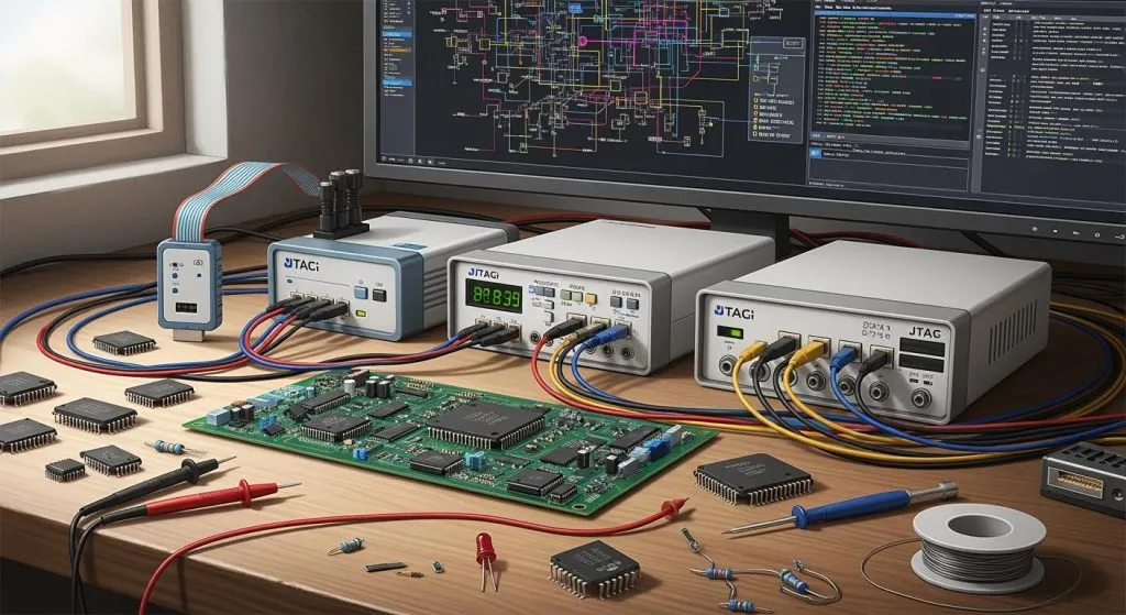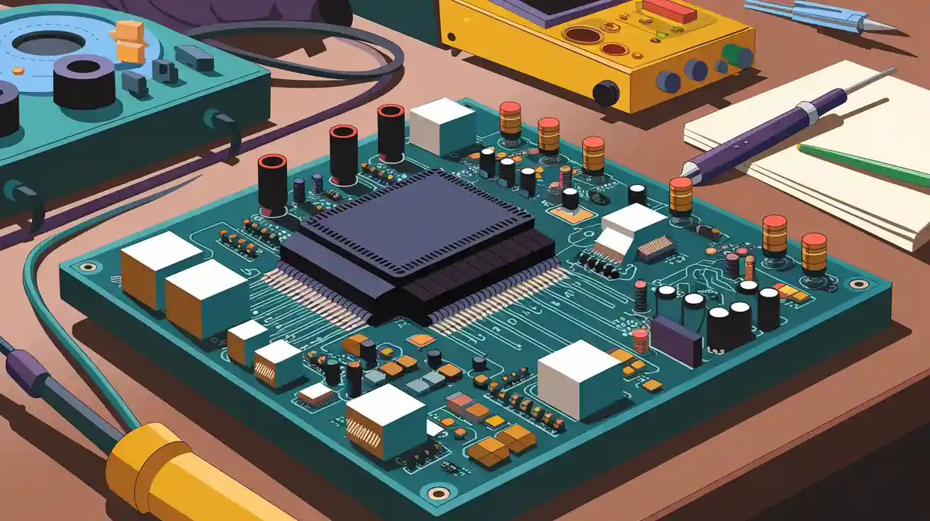
Designing an amplifier PCB is more than joining parts. A good layout makes the amplifier work well and last long. Beginners may struggle with wrong models or skipping checks. These mistakes can cause problems with how it works or lasts. Using simple tips can help avoid these issues. Planning carefully and focusing on details will make a strong and reliable amplifier PCB.
Key Takeaways
A good layout is very important for amplifier PCBs. It helps them work better and last longer.
Keep wires short and avoid sharp turns to keep signals clear and reduce noise.
Place decoupling capacitors near chips to steady voltage and lower electrical noise.
Use a solid ground layer to make the circuit stable and block bad signals.
Handle heat well with heat sinks and thermal holes to stop damage and keep it working.
Understanding Amplifier PCB Basics
What is an Amplifier PCB
An amplifier PCB is a board that boosts electrical signals. It organizes and connects parts to make signals stronger. The design depends on the signal’s frequency range. For example:
In MHz signals, input impedance and part properties matter most.
For higher frequencies, impedance matching and stripline design are key.
Amplifiers are grouped by how they connect signals:
RC-coupled amplifiers work for AC signals but not DC signals.
LC-coupled amplifiers are great for RF circuits.
Transformer-coupled amplifiers match signal strength well.
Direct-coupled amplifiers are common in modern devices.
One example is a class-AB amplifier, which uses feedback to improve. Another example is an RF amplifier that works at 6 GHz and gives +13 dB gain.
Key Components in an Amplifier PCB
An amplifier PCB has important parts that amplify signals:
Amplification Unit: Transistors or op-amps make signals stronger.
Resistors: Control current and adjust the amplifier’s power.
Capacitors: Filter signals and keep voltage steady.
Inductors: Remove unwanted high-frequency noise.
Power Supply Unit (PSU): Provides stable power to the circuit.
Input and Output Terminals: Connect the source and send signals out.
Heat Sinks: Cool down circuits that use a lot of power.
Printed Traces: Link parts while keeping signals clean.
Choosing and placing these parts carefully ensures the amplifier works well.
Basic Principles of PCB Design for Amplifiers
Follow these rules to design a good amplifier PCB:
Keep connections to the inverting pin very short.
Place decoupling capacitors close to supply pins. Use small ones first.
Avoid vias between capacitors and supply pins.
Use wide traces to improve current flow.
Don’t route traces at sharp angles to avoid signal problems.
Add a solid ground plane to reduce noise and improve stability.
Focus on layout quality over labeling for better signal strength.
These steps help create a strong and efficient amplifier PCB.
Common Mistakes in Amplifier PCB Design
Poor Component Placement
Putting parts in the wrong spots can cause big problems. It may lead to noise, instability, or even broken circuits. Plan the layout carefully to avoid these issues. Here are some examples of bad placement and their effects:
A high-frequency op-amp had issues above 100 MHz. Long traces caused stray capacitance and oscillations. Shorter traces and a compensation capacitor fixed it.
In a mixed-signal circuit, digital noise affected analog parts. Separating and arranging them properly reduced the noise.
An automotive motor drive failed EMI tests. Long traces between MOSFETs and the gate driver caused noise and high EMI. Shorter traces solved the problem.
To prevent these problems, group related parts together. Keep trace lengths short. Separate analog and digital sections to reduce noise. Good placement improves performance and reliability.
Ignoring Signal Integrity and Noise Reduction
Signal integrity is very important for amplifier PCBs. Ignoring it can cause noise, crosstalk, and signal problems. For example:
Bad signal integrity makes it hard to read logic levels in fast circuits.
Crossing splits in ground or power planes increases noise and crosstalk. This lowers signal quality.
High-speed signals can act like transmission lines. This changes how signals behave.
To keep signals clean, avoid crossing plane splits. Keep high-speed traces short and straight. Use proper termination to stop reflections. These steps reduce noise and keep signals clear.
Overlooking Thermal Management
Managing heat is crucial for amplifier PCBs. Too much heat can lower performance or break parts. Important heat-related factors include:
Metric | What It Means |
|---|---|
Thermal Resistance | Shows how well heat moves away from parts. |
Maximum Junction Temperature | The highest temperature a part can handle before breaking. |
Impact on Device Reliability | High heat can shorten lifespan and cause serious problems. |
Ignoring heat management can cause overheating. This affects how transistors work and lowers reliability. Use heat sinks, thermal vias, and good materials to remove heat. Check thermal resistance and stay within safe temperature limits.
Tip: Watch power-hungry parts like transistors and MOSFETs. Good heat management keeps your amplifier working well and lasting longer.
Skipping Good Grounding Practices
Grounding is very important in amplifier PCB design. Bad grounding can cause noise, unstable circuits, or even failure. A good grounding system blocks unwanted signals and keeps the circuit working well.
Ignoring grounding can lead to problems. For example, a high-impedance ground plane makes EMI and RFI worse. This lowers signal quality and hurts performance. Using a buss wire for grounding causes voltage drops. These drops create errors in signal processing. Mixing digital and analog return currents also creates error voltages. This adds noise and reduces accuracy in your amplifier.
Here’s how bad grounding affects amplifiers:
Grounding Problem | Effect on Amplifier Performance |
|---|---|
Low-impedance ground plane reduces EMI/RFI | Improves signal quality and blocks outside noise |
Buss wire grounding causes voltage drops | Leads to errors and lowers signal processing quality |
Digital currents mixing with analog currents | Adds noise and reduces amplifier accuracy |
To fix these issues, use a low-impedance ground plane. This cuts down EMI and RFI, keeping signals clean. Separate digital and analog grounds to stop interference. Add grounding vias to give return currents a direct path. These steps make your amplifier more reliable and work better.
Tip: Check your grounding design carefully. Small mistakes can cause big problems later.
Step-by-Step Guide to Designing an Amplifier PCB
Make a Schematic Diagram
The schematic diagram is the first and most important step. It acts like a map, showing how parts connect and work together. Following clear steps helps avoid mistakes during design. Here’s how to make a good schematic:
Component Placement: Place parts in order from input to output. This makes the circuit easy to follow and fix.
Ground Plane Design: Use a solid ground plane to block EMI and keep signals clean.
Trace Routing: Keep traces short to avoid unwanted effects like noise.
Power Supply Decoupling: Put small capacitors near power pins to reduce noise.
Signal Integrity: Protect signal lines by adding grounded traces nearby.
Thermal Management: Add vias under hot parts to help remove heat.
Testing and Prototyping Considerations: Add test points to make debugging easier.
Pro Tip: Check your schematic for missing links or wrong polarities. Fixing small errors now avoids big problems later.
Pick the Right PCB Design Software
Choosing the right software is key for making a good amplifier PCB. The software should match your skill level and project needs. Think about these points when picking software:
Hobbyist vs. Professional Software: Beginners can use tools like KiCad or EasyEDA. These are simple and have helpful guides. Experts may prefer Altium Designer or Eagle for advanced features.
Efficiency and Precision: Good software saves time with templates and 3D views. These tools help reduce mistakes and wasted materials.
Cost Savings: Digital tools let you edit designs without wasting physical materials.
Did You Know? Surveys show that good software improves PCB design success. Picking the right tool makes your work faster and better.
Set Board Size and Layers
Setting the board size and layers is very important. The PCB’s size and layers affect how it works, costs, and gets made. Follow these tips to start:
Size Standards | Layer Setup |
|---|---|
IPC-2221 rules guide board spacing and clearances. | A four-layer board includes: Copper Top, Inner 1, Inner 2, Copper Bottom. |
Common PCB thicknesses are:
.031”
.062” (most popular size)
.093”
.125”
Think about the amplifier’s power needs and space in your device. For multi-layer boards, stack layers well to improve signals and heat control.
Tip: Use a four-layer board for tricky designs like instrumentation amplifiers. This setup gives better grounding and reduces noise.
Strategically Place Components
Placing parts smartly on your amplifier PCB helps it work better. It also reduces problems like noise or interference. Follow these simple tips for a clean layout:
Group Related Components Together: Keep parts that work together, like resistors and capacitors, close. This shortens traces and keeps signals strong.
Separate Analog and Digital Sections: Put analog parts away from digital ones. This stops digital noise from messing with analog signals.
Position Noise-Generating Components Carefully: Noisy parts like regulators or oscillators should be far from sensitive circuits. This avoids unwanted signals.
Use Proper Orientation: Line up parts to stop signals from mixing. This lowers crosstalk and keeps signals clear.
Tip: Place decoupling capacitors near IC power pins for RF immunity. Use different capacitor values to block many frequencies. Short, wide traces for power and ground also cut noise.
Studies show good part placement improves performance in home and car amplifiers. Separating analog and digital parts reduces interference in automotive audio systems.
Route Traces and Connections
Routing traces well is key for a good amplifier PCB. It keeps signals clean and reduces noise. Use these tips for better routing:
Best Practice | What to Do |
|---|---|
Controlled Impedance | Keep impedance steady for high-speed signals to avoid distortion. |
Minimize Crosstalk | Space out traces to stop signals from mixing. |
Proper Grounding | Use one solid ground plane for better performance. |
Avoid Hot Spots | Add vias in a grid to spread current evenly. |
135° Trace Bends | Use 135° bends instead of sharp 90° ones for better signal flow. |
Daisy Chain Routing | Avoid long stubs to keep signals clear. |
Differential Pair Routing | Keep paired traces close to reduce noise. |
Length Matching | Match trace lengths for signals that need to arrive together. |
Note: High-frequency signals need short, straight traces. Keep them away from noisy parts like power lines. Guard traces around important signals can also help.
By following these tips, your amplifier PCB will work well in different conditions.
Add Ground Planes and Power Distribution
Adding ground planes and good power distribution makes your amplifier PCB stable. Ground planes give signals a steady base, and power planes keep voltage even. Here’s how to do it:
Ground Planes: Use a solid ground plane to cut noise and keep signals steady. Close power and ground planes act as shields, blocking EMI. They also help return currents stay consistent.
Power Planes: Use a power plane to spread power evenly. This lowers noise and gives all parts steady voltage. Power planes also help cool the board.
Thermal Management: Ground and power planes help remove heat. This stops overheating and makes parts last longer.
Pro Tip: Replace thin, long traces with solid planes to lower power noise. This boosts your amplifier PCB’s performance.
Tests show solid planes reduce noise and improve heat control. This is vital for high-speed designs needing stability and cooling.
Perform Design Rule Checks (DRC)
Design Rule Checks (DRC) help ensure your amplifier PCB design is correct. These checks find mistakes that could cause problems during production or use. Running DRC early saves both time and money.
Why DRC is Important
Skipping DRC can lead to broken circuits or bad performance. For example, traces placed too close might cause short circuits. Pads that are the wrong size can make soldering difficult. DRC helps your design meet industry rules and avoids these issues.
Steps to Perform DRC
Follow these steps to check your design:
Set Design Rules: Use your manufacturer’s guidelines for trace width, spacing, and vias.
Run Automated Checks: Use software like KiCad or Altium Designer to scan for errors.
Review Errors: Look at flagged issues. Some may not matter, but others need fixing.
Fix Problems: Adjust your design to solve errors, like resizing pads or spacing traces.
Recheck the Design: Run DRC again to confirm all problems are fixed.
Tip: Always follow your manufacturer’s rules when setting design limits. This ensures your PCB is ready to be made.
Common DRC Errors to Watch For
Here are some common errors you might see:
Trace Spacing Issues: Traces too close can cause short circuits.
Pad Size Problems: Small pads can make soldering harder.
Unconnected Nets: Missing links can stop the circuit from working.
Overlapping Parts: Components placed too close can interfere with each other.
Fixing these errors makes your PCB more reliable and better performing.
Prepare the PCB for Manufacturing
Getting your amplifier PCB ready for manufacturing is very important. These steps make sure your design is correct and easy to produce. Good preparation reduces mistakes and ensures smooth production.
Steps to Prepare Your PCB
Here’s how to get your PCB ready:
Generate Gerber Files: Export your design into Gerber files. These files tell manufacturers how to build your PCB.
Check Manufacturer Capabilities: Make sure your manufacturer can handle your design, like board size or layers.
Confirm Schematic Design: Double-check your schematic for correct connections and labels.
Pick Materials: Choose materials based on your amplifier’s needs, like FR4 for high-frequency designs.
Submit Design for Review: Share your design with the manufacturer. They may suggest changes to improve it.
Note: Many manufacturers offer free reviews to help improve your design.
Quality Control Standards
Quality checks ensure your PCB meets industry standards. Here are some practices:
IPC-A-600 explains the minimum quality needed for PCBs.
Manufacturers with IPC certifications show they care about quality.
Quality control includes checking manufacturer abilities and confirming schematics.
Final Checklist
Before sending your PCB for production, review this list:
✅ Gerber files are complete and correct.
✅ Design rules match manufacturer guidelines.
✅ Materials fit your amplifier’s needs.
✅ Schematic is error-free.
✅ Manufacturer has approved the design.
By following these steps, your amplifier PCB will be ready for production and meet high standards.
Pro Tip: Stay in touch with your manufacturer. Their advice can help you avoid mistakes and improve your design.
Best Practices for Amplifier PCB Layout

Optimize Trace Width and Length
Making trace width and length right is key for your amplifier PCB to work well. Wider traces let more current flow and stop overheating. The IPC-2221 rule helps you design to meet industry standards. It gives a formula to find the right trace width based on current, so you avoid voltage drops or broken traces.
When planning your PCB layout, think about these important points:
Impedance is crucial in fast circuits. Keeping it steady stops signal bouncing and keeps signals clear.
Wider traces spread heat better, helping with heat control.
Narrow traces can get too hot with high current, causing damage.
To make trace width and length better, do these steps:
Use the IPC-2221 formula to find the trace width you need, thinking about the current load.
Keep traces short to lower resistance and voltage drop.
Consider the board material and outside temperature, as they affect heat spreading.
Tip: Make power and ground traces as wide as you can. This cuts noise and makes your amplifier more stable.
Use Decoupling Capacitors Effectively
Decoupling capacitors are super important for keeping your amplifier PCB steady. They give charge to ICs and keep low impedance between power and ground. This cuts down on electromagnetic interference (EMI) and keeps things running smoothly.
To use decoupling capacitors best, follow these tips:
Put decoupling capacitors really close to IC power pins. This stops voltage changes and cuts electrical noise.
Use capacitors with different values to filter many frequencies. For example, mix a 0.1 µF capacitor with a 10 µF one to handle both high and low-frequency noise.
Make sure decoupling capacitors are placed right and have the correct polarity to avoid problems.
Decoupling capacitors also help during quick voltage changes. They keep voltage levels steady, stopping signal problems and protecting sensitive parts.
Pro Tip: If there’s room, put decoupling capacitors on both sides of the PCB. This boosts EMI blocking and makes your amplifier work better.
Implement Proper Grounding and Shielding
Good grounding and shielding cut noise and keep your amplifier PCB stable. A solid ground plane gives a low-impedance path for return currents and blocks electromagnetic interference.
Here are some good ways to ground and shield:
Technique | Description |
|---|---|
Metal Enclosure | Works like a Faraday cage, shielding the circuit from outside EMI. Good grounding stops ground loops. |
Conductive Coating | Adds a metal layer, like copper or nickel, to block electromagnetic waves. |
Shielded Cables | Cuts noise by wrapping wires in a metal shield. Grounding the shield at both ends makes it work better. |
A study on stopping EMI showed how power line and ground filters fix tough interference problems. Good grounding and shielding make sure your amplifier works well in places with lots of electromagnetic activity.
To use these methods:
Use a full ground plane to lower impedance and improve signal quality.
Don’t split the ground plane, as this can make noise and hurt performance.
Shield sensitive parts with metal covers or conductive coatings to block outside interference.
Note: Always connect the shield to the ground at one spot to stop ground loops, which can add more noise.
Reduce Noise and Interference
Noise can harm how your amplifier works. To keep signals clear, use methods to lower unwanted noise in your PCB design. Here are some simple ways:
Arrange Components Smartly
Keep analog and digital parts in separate areas. This stops digital noise from affecting sensitive analog signals. Make signal paths short to avoid picking up extra noise.
Use Good Trace Routing
Avoid sharp turns like 90-degree angles in traces. These can cause signal problems and more noise. Use 45-degree or smooth curves instead. For fast signals, try differential pairs. They cancel out noise by carrying opposite signals.
Add Shields and Isolation
Metal cases and shields on the PCB block outside noise. Adding a conductive layer to the PCB surface also helps. These are useful in places with lots of electromagnetic activity.
Use Filters
Filters remove unwanted frequencies. Low-pass filters block high-frequency noise. High-pass filters stop low-frequency noise. Band-pass and notch filters focus on specific ranges, letting only needed signals through.
Test for Noise
Use tools like spectrum analyzers or oscilloscopes to check noise levels. These tools help find noisy spots and confirm your design works well.
The table below shows ways to reduce noise and interference:
Strategy Type | Techniques |
|---|---|
Component Layout | – Separate analog and digital circuits |
– Keep signal paths short | |
Trace Routing | – Avoid sharp angles |
– Use differential pairs | |
Shielding | – Use metal cases |
– Add PCB shields | |
Filtering | – Use low-pass, high-pass, or band-pass filters |
Testing Tools | – Use spectrum analyzers and oscilloscopes |
By following these tips, your amplifier will have cleaner signals and work better.
Manage Heat Effectively
Heat can damage your amplifier if not handled well. Good thermal management keeps it running smoothly and safely.
Use Heat Sinks and Vias
Heat sinks pull heat away from hot parts like transistors. Attach them directly to these parts. Thermal vias, small holes with metal, move heat between PCB layers.
Improve Ground and Power Planes
Ground and power planes spread heat evenly. A solid ground plane stops hot spots. Make sure these planes are big enough to handle heat.
Pick the Right Materials
The PCB material affects heat control. FR4 is common, but for hotter amplifiers, use materials like metal-core PCBs. These spread heat better.
Check Thermal Resistance
Thermal resistance shows how well heat leaves a part. Lower resistance means better cooling. Check this for all parts to stay within safe limits.
Allow Airflow
If your amplifier is in a closed space, make sure air can move around. Place parts to allow airflow. Add fans or vents for extra cooling.
The table below lists ways to manage heat:
Technique | Description |
|---|---|
Heat Sinks | Pull heat away from hot parts. |
Thermal Vias | Move heat between PCB layers. |
Ground and Power Planes | Spread heat evenly to stop hot spots. |
High-Thermal Materials | Use materials like metal-core PCBs for better heat control. |
Airflow Design | Allow air to flow or add fans for cooling. |
By using these heat management tips, your amplifier will last longer and work reliably.
Making an amplifier PCB needs careful planning and focus on details. A good layout helps it work better and last longer. By using the tips in this guide, you can avoid errors. Follow steps like good grounding, cutting noise, and managing heat. Trying out PCB design tools will improve your skills over time. Begin with simple projects and learn from each one. Slowly, you can handle harder designs. With practice, you’ll get better at building strong and efficient amplifier PCBs.
FAQ
What is the best PCB design software for beginners?
Start with KiCad or EasyEDA. These are free and simple to use. They include tutorials and templates to guide you. For advanced features, try Altium Designer or Eagle later.
How do I calculate the correct trace width?
Use the IPC-2221 standard formula. It factors in current, copper thickness, and heat rise. Online tools like PCB Trace Width Calculator make this easier. Wider traces carry more current and stay cooler.
Why is grounding so important in amplifier PCB design?
Grounding keeps signals stable and reduces noise. A solid ground plane gives return currents a low-impedance path. This boosts performance and blocks electromagnetic interference (EMI).
How can I reduce noise in my amplifier PCB?
Separate analog and digital parts. Use short, straight traces without sharp turns. Place decoupling capacitors close to ICs. Shield sensitive areas with metal covers or coatings.
What materials should I use for high-power amplifier PCBs?
For high-power designs, use FR4 for general needs or metal-core PCBs for better heat control. Metal-core materials handle heat well and improve cooling.
Tip: Ask your manufacturer for advice on materials for your design.