What is the PCB Fabrication Process?

As the carrier of electronic components, PCB plays a vital role in the electronics manufacturing industry. Its production process is complex and precise, directly affecting the performance and quality of the final product. WonderfulPCB, a trusted SMT processing factory, provides a detailed analysis of the PCB production process to help electronics manufacturers and procurement teams better understand it.

Overview of the PCB Production Process

The PCB production process can be divided into several key stages: inner layer fabrication, lamination, drilling, metallization, outer layer fabrication, surface protection, and final inspection and packaging. Each step involves various techniques and technologies, requiring a high degree of precision and expertise.

Inner Layer Fabrication

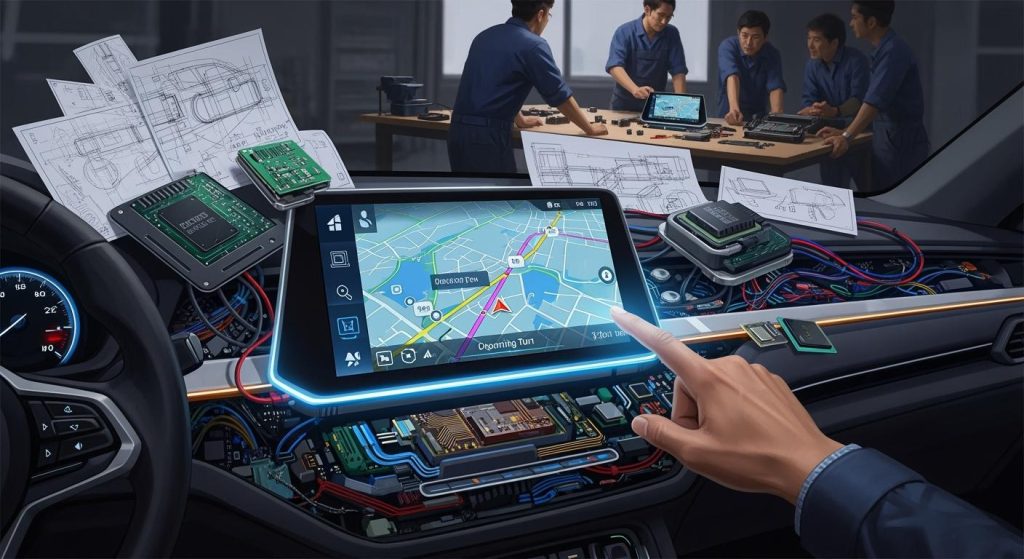
The inner layers are the core of the PCB, connecting the electronic components. The process includes:

Copper-clad plate cutting

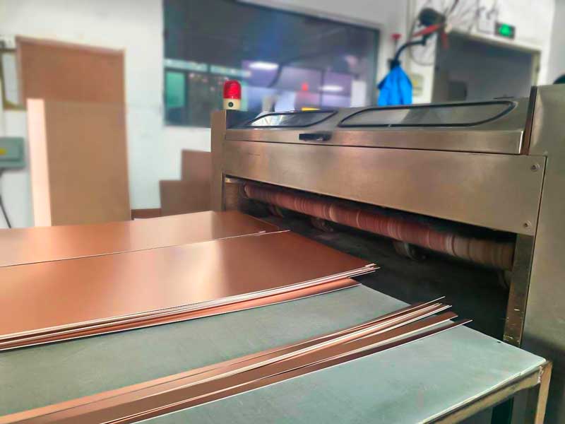
  • Board Cutting: Cutting the original PCB substrate to the required size for production.
  • Pre-treatment: Cleaning the substrate surface to remove oil, oxides, and other contaminants, ensuring smooth progress in subsequent steps.
  • Lamination: Applying a layer of dry film to the substrate’s surface, which will transfer the circuit pattern during exposure.
  • Exposure: Using ultraviolet light to expose the laminated board, transferring the designed circuit pattern onto the dry film.
  • Developing, Etching, and Stripping: Removing the unexposed areas of the dry film through development, then etching away the unprotected copper layer, and finally removing the remaining dry film to form the inner layer circuit.
  • AOI (Automated Optical Inspection): Checking the quality of the inner layer circuit to ensure there are no open circuits, shorts, or other defects.

Lamination

Lamination combines multiple inner layers into one multilayer board using resin materials. This step is critical for multilayer PCBs, and the process includes:

  • Brown Oxide: Increasing adhesion between the layers and improving the wettability of the copper surface.
  • Stacking: Layering the inner circuits and PP (Prepreg) sheets according to design requirements.
  • Pressing: Applying high temperature and pressure to bond the layers into a single multilayer board.
  • Target Drilling, Routing, and Edge Grinding: Trimming the laminated board to remove excess material and achieve the design dimensions.

Drilling

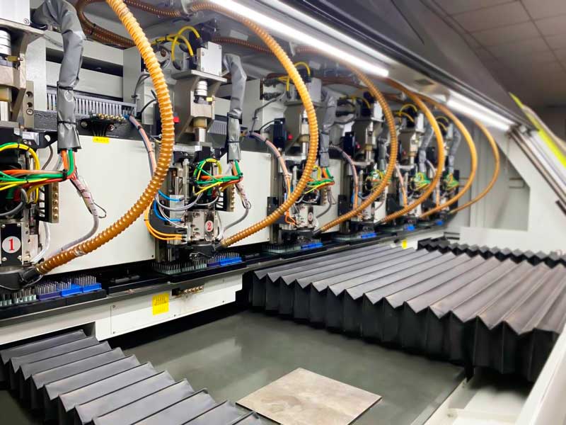
Drilling is necessary to create through holes or blind holes for electrical connections and component installation. The process includes:

  • Drilling: Using a drilling machine to create holes according to design specifications.
  • Deburring: Removing burrs formed during drilling to ensure smooth hole walls.

PCB drilling

Hole Metallization

In this step, a thin layer of copper is deposited on the insulating hole walls to create a conductive base for further copper plating. The process includes:

  • PTH (Plated Through Hole) Copper Deposition: Chemically depositing a copper layer on the hole walls.
  • Hole Filling: Plating copper inside the holes to create a complete conductive path.

Outer Layer Fabrication

The outer layer fabrication is similar to the inner layers but more complex, as it involves forming the circuit pattern on the outer layers of the multilayer PCB. The steps include:

  • Outer Layer Pre-treatment: Cleaning the outer surface to remove contaminants.
  • Lamination, Exposure, and Developing: Forming the outer layer circuit pattern by lamination, exposure, and developing, similar to the inner layer process.
  • Pattern Plating: Electroplating copper onto the circuit pattern to thicken the traces.
  • Stripping, Etching, and Tin Stripping: Removing the dry film, etching away unprotected copper, and stripping off the tin layer to reveal the final outer layer circuit.

Surface Protection

Surface protection prevents oxidation and corrosion of the circuit while improving solderability. The steps include:

  • Solder Mask: Applying a layer of photo-sensitive solder mask ink, followed by exposure and developing to form a solder mask that protects the circuit from soldering.
  • Surface Treatment: Methods such as electroless nickel/immersion gold (ENIG) are used to enhance solderability and corrosion resistance.
  • Silkscreen Printing: Printing text and identification symbols on the board for easier assembly and maintenance.

Final Inspection and Packaging

Final inspection ensures PCB quality, including AOI inspection, flying probe testing, and ensuring there are no shorts or opens. Once the boards pass inspection, they are vacuum-packed, packaged, and shipped for delivery.