Introduction
Flexible printed circuit boards (FPC) and Rigid-Flex printed circuit boards demonstrate advanced circuit board technology that twists, bends and folds to fit unique product designs. You find these bendable circuit boards everywhere in modern electronics, smartphones, wearables, medical devices, and automotive systems. Their ability to adapt to three-dimensional shapes and survive millions of flex cycles makes them irreplaceable in compact, high-reliability applications.
Companies need PCB cloning services for several significant reasons. You lost your original design files when a key engineer quit. Your OEM discontinued production, leaving you without replacement boards. Supply chain issues forced you to find alternative manufacturing sources. You need to redesign or upgrade legacy products while maintaining compatibility. These situations demand precise flexible PCB cloning to keep your products in production.
Cloning flexible and rigid-flex PCBs needs specialized reverse engineering skills far beyond standard rigid board cloning. The unique materials, complex layer structures, and critical bend area designs demand advanced technical capabilities and experience. This guide shows you the complete process, technical challenges, and what to obtain when cloning bendable circuit boards.
What Is Flexible PCB Cloning?
Flexible PCB reverse engineering rebuilds your original circuit board design from a physical sample when you lack manufacturing files. You provide the existing flexible PCB. We analyze every aspect material, layer structure, trace routing, component placement, and mechanical properties. The process delivers complete manufacturing-ready documentation.
Files recreated during flexible PCB cloning include Gerber files defining all copper layers and features, complete PCB stack-up documentation specifying materials and thicknesses, full BOM (Bill of Materials) listing all components with specifications, and schematic diagrams showing electrical connections and circuit functionality. These files enable exact reproduction or redesign of your flexible PCB.
Flexible PCB cloning differs significantly from rigid PCB cloning. You analyze polyimide or polyester substrate instead of FR-4. Coverlay swaps solder mask. Rolled annealed copper behaves differently than standard copper. Bend areas need special design analysis.
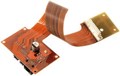
| Figure 1 A Typical Flexible PCB |
Industries that use flexible PCBs widely include consumer electronics (smartphones, tablets, cameras), wearable technology (smartwatches, fitness trackers, health monitors), medical devices (hearing aids, pacemakers, surgical instruments), automotive electronics (dashboard displays, sensor connections, lighting systems), and aerospace applications (satellite systems, avionics, space-constrained installations).
What Is Rigid-Flex PCB Replication?
Rigid-Flex PCBs merge rigid board sections with flexible interconnects in a single integrated assembly. The structure alternates between rigid FR-4 layers for component mounting and flexible polyimide sections for movement and 3D packaging. Multi-layer stack ups can include 4, 6, 8, or more layers with complex transitions between rigid and flex zones. Specialized lamination processes bond these dissimilar materials together reliably.
Rigid-Flex cloning is more complex than standard FPC reverse engineering. You must identify where rigid sections end and flex sections start. Layer count changes between zones. Some layers continue through the entire board while others stop at transition zones. Via structures vary, through-hole vias in rigid areas, potentially blind or buried vias at transitions. This complexity demands experienced engineering analysis.
Engineering challenges include layer stack identification determining which layers exist in each zone, flex bend area design analysis ensuring proper stress relief and reliability, coverlay and adhesive material recognition matching original specifications, and controlled impedance structures maintaining signal integrity across rigid-flex transitions. Each challenge needs dedicated knowledge to solve properly.
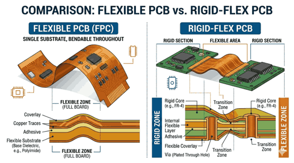
| Figure 2 Comparison showing Flexible PCB versus Rigid-flex PCB |
Technical Challenges in Flexible & Rigid-Flex PCB Cloning
1. Material Identification
Polyimide thickness analysis identifies the exact substrate specification i.e. 12.5µm, 25µm, 50µm, or other thicknesses. This affects flexibility and electrical properties. Copper weight measurement identifies whether you have 0.5oz, 1oz, or 2oz copper, and whether it is rolled annealed (RA) or electro-deposited (ED) type. Adhesive and coverlay detection shows bonding methods and protective layer specifications. Surface finish identification determines whether you have ENIG, OSP, immersion silver, or other finishes.
2. Layer-by-Layer Structural Analysis
Mechanical cross-sectioning cuts through the printed circuit board to represent internal layer structure. You examine how many layers exist, their arrangement, and material interfaces. Microscopic imaging takes high-resolution photographs of each layer showing trace patterns, via structures, and material boundaries. X-ray inspection for inner layers shows buried structures invisible to optical inspection. Via structure mapping documents all connection points between layers including blind vias and buried vias in complex designs.
3. Bend Area Reliability Assessment
Dynamic bending fatigue considerations confirm the cloned design endures repeated flexing cycles. You analyze copper hatching patterns that reduce stiffness, teardrop pad designs that avoid stress concentration, and trace routing perpendicular to bend axis. Stress concentration areas receive specific attention. You detect anchor points, stiffener locations, and radius requirements. Design reinforcement analysis observes how the original board operates mechanical stress to keep reliability.
IC Protection & Firmware Extraction
Microcontroller read protection levels clarify accessibility of firmware code. Encrypted chip handling needs specialized techniques when components use security features. Firmware backup becomes necessary when you need complete system functionality reproduction. This service continues only with proper approval, authorization and ownership documentation, maintaining strict compliance with intellectual property laws and industry regulations.

| Figure 3 Multilayer Flexible PCB showing polyimide substrate, copper traces, and coverlay |
Flexible & Rigid-Flex PCB Cloning Process
Step 1: Initial PCB Inspection & Documentation
High-resolution photography captures every detail of both sides of your flexible printed circuit board. Component mapping recognizes and documents all parts including ICs, passives, connectors, and mechanical components. Functional testing, when applicable verifies the board works accurately and determines baseline performance for comparison after cloning.
Step 2: PCB Dis-assembly & Layer Separation
Controlled grinding removes layers sequentially without damaging underlying structures. Layer imaging photographs show each displayed layer before removal. Trace reconstruction maps all copper patterns, via locations, and pad geometries. This detailed process represent the complete internal structure of multilayer flexible or rigid-flex circuit boards.
Step 3: Schematic Reconstruction
Circuit tracing follows all electrical connections between components. Signal path analysis identifies essential traces involving impedance control or special routing. Power and grounding structure rebuilding recreates the voltage distribution network and ground planes. The resulting schematic shows complete circuit functionality.
Step 4: Gerber & Manufacturing File Generation
DFM (Design for Manufacturing) optimization ensures the design obtains production capabilities and quality standards. Stack-up documentation indicates all materials, thicknesses, and layer arrangement. Drill files and fabrication drawings provide complete manufacturing instructions including tolerances, bend radius requirements, and stiffener placement.
Step 5: Prototype Manufacturing & Assembly
Flexible PCB fabrication produces prototypes using the exact materials and processes identified during reverse engineering. Rigid-Flex PCB manufacturing processes the complex lamination and processing required for combined structures. SMT assembly organizes all components using precision equipment. Component sourcing support track current equivalents for outdated parts when necessary. This full-service capability takes you from reverse engineering through final tested assemblies.
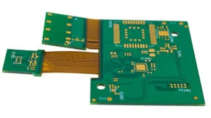
| Figure 4 Typical Rigid Flex PCB |
Applications of Flexible & Rigid-Flex PCB Cloning
Wearable electronics require flexible PCBs that follow to body contours and survive constant movement. You clone fitness tracker circuits, smartwatch interconnects, and health monitoring sensor boards when original designs become unavailable.
Medical devices depend on flexible circuits for compact, reliable designs. You reverse engineer hearing aid circuits, pacemaker interconnects, surgical instrument controls, and patient monitoring systems. Regulatory compliance needs exact reproduction of proven designs.
Automotive electronics use rigid-flex PCBs behind dashboards, in door modules, and throughout modern vehicles. You clone discontinued control modules, sensor connections, and display interfaces to maintain vehicle production or provide replacement parts.
Industrial control systems incorporate flexible circuits in rotating machinery, moving arms, and space-constrained installations. Consumer electronics including cameras, drones, and gaming devices use flexible interconnects extensively. Aerospace applications demand high reliability rigid-flex designs for avionics, satellite systems, and serious flight controls where failure is not tolerable.

| Figure 5 Flexible PCB applications |
Flexible vs Rigid-Flex PCB Cloning: Key Differences
Understanding the differences helps you set realistic expectations for your project:
| Factor | Flexible PCB | Rigid-Flex PCB |
| Structural Complexity | Single substrate type | Multiple zones, transitions |
| Reverse Engineering Difficulty | Moderate | High |
| Manufacturing Difficulty | Standard flex process | Complex lamination |
| Typical Applications | Wearables, simple interconnects | Medical, aerospace, automotive |
| Turnaround Time | 7-12 days | 12-20 days |
Why Choose a Professional Flexible PCB Reverse Engineering Company?
Experience with multi-layer flexible boards matters critically. You need engineers who have reverse engineered hundreds of flexible and rigid-flex PCBs designs across multiple industries. They identify common design patterns, understand material behaviors, and predict potential issues before they become problems.
Advanced inspection equipment including high-resolution microscopes, X-ray imaging systems, and precision measurement tools enables accurate analysis. In-house PCB manufacturing capabilities eliminate coordination issues between reverse engineering and production teams. SMT production lines allow complete assembly services from bare boards to tested final products.
Strict NDA and IP protection safeguards your proprietary designs. You receive ironclad confidentiality guarantees before sharing your boards. Fast prototype turnaround develops your replacement boards quickly when production cannot wait.
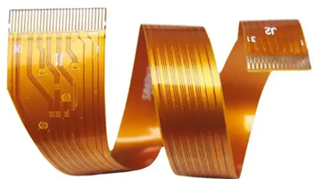
| Figure 6 Flexible PCB Reverse Engineering |
Frequently Asked Questions
Can a damaged flexible PCB be cloned?
Yes, damaged flexible PCBs can be cloned in most cases. Minor damage like torn flex sections, missing components, or surface scratches does not avoid reverse engineering. We reconstruct missing or damaged areas by analyzing intact sections and applying standard design practices.
Is firmware extraction possible from protected MCUs?
Firmware extraction from protected microcontrollers is possible for many devices using expert techniques including fault injection, glitching, and debug interface exploitation. Success rates exceed 80% for common MCUs with standard read protection.
Do you provide manufacturing after cloning?
Yes, we provide complete manufacturing services after reverse engineering. Our in-house flexible PCB and rigid-flex PCB production lines handle fabrication.
Is flexible PCB cloning legal?
Flexible PCB cloning is legal when you own the boards or have explicit permission from the owner. Legitimate uses include replacing discontinued products, maintaining legacy equipment, recovering lost design files, and supporting products you manufacture or service. We need ownership documentation or authorization letters before accepting projects.
Conclusion
Meticulousness in flexible and rigid-flex PCB cloning decides whether your replacement boards work reliably or fail instantly. Material specifications must match exactly. Layer structures require perfect recreation. Bend areas need proper stress relief design. These details separate successful cloning from expensive failures.
Technical capability combined with full-service support gives results you can expect. You work with experienced engineers who understand flexible circuit design closely. Advanced equipment shows internal structures correctly. In-house manufacturing ensures seamless progression from reverse engineering to production. Complete assembly expertise provide tested boards ready for installation.
Ready to clone your flexible or rigid-flex PCB? Submit clear photos of both sides of your circuit board for evaluation. We evaluate complexity, provide detailed quotes, and outline realistic timelines. Our team stands ready to solve your flexible PCB challenges with proven expertise and complete manufacturing support.
Contact Wonderful PCB Today:
Email: [email protected]
Phone: +86 0755-86229518
Visit: www.wonderfulpcb.com