The assembly quality of SMT (Surface Mount Technology) is directly related to the PCB pad design, and the size ratio of the pads is crucial. If the PCB pad design is correct, minor misalignment during placement can be corrected during the reflow soldering process (known as self-alignment or self-correction effect). On the other hand, if the PCB pad design is incorrect, even precise placement can result in component misalignment, solder bridges, and other soldering defects after reflow soldering.
Basic Principles of PCB Pad Design
Based on the analysis of various component solder joint structures, to ensure the reliability of the solder joints, the PCB pad design should focus on the following key factors:
- Symmetry: The pads at both ends must be symmetric to ensure the balance of the molten solder’s surface tension.
- Pad Spacing: Ensure the proper overlap between the component leads or pins and the pads. Pads that are too far apart or too close together can cause soldering defects.
- Remaining Pad Size: The remaining size after the component lead or pin overlaps with the pad must be sufficient to allow for the formation of a reliable solder joint.
- Pad Width: The pad width should generally match the width of the component lead or pin.
Solderability Defects Caused by Pad Size
Inconsistent Pad Sizes
Pad sizes must be consistent, and their length should be within an appropriate range. Pads that are too short or too long can cause the “tombstoning” (standing up) phenomenon. Inconsistent pad sizes or uneven pull forces can also lead to component tombstoning.
Pad Width Too Wide Compared to Component Leads
The pad design should not be excessively wide compared to the component. A pad width that is two mils wider than the component lead is sufficient. If the pad width is too wide, it can lead to component displacement, cold solder joints, or insufficient solder coverage on the pad.

Pad Width Too Narrow Compared to Component Leads
If the pad width is narrower than the component lead, there will be insufficient contact area between the component lead and the pad during SMT placement. This can cause the component to tilt or flip during the soldering process.

Pad Length Too Long Compared to Component Leads
Pads should not be excessively long compared to the component leads. If the pad extends too far, excessive solder paste flow during reflow soldering can pull the component to one side, causing misalignment.

Pad Spacing Too Close
The issue of short-circuiting due to insufficient pad spacing typically occurs in IC pads. However, the inner spacing of pads for other components should not be significantly shorter than the lead spacing of the component. If the spacing is too narrow, it can also result in a short circuit.
(pic-PCB Pad Design-4)
Pad Pin Width Too Small
In SMT placement, if a pad width is too small, it can lead to misalignment. For example, if a particular pad is too small or some pads are smaller than others, it can result in insufficient or no solder on that pad, causing uneven tension and displacement of the component.

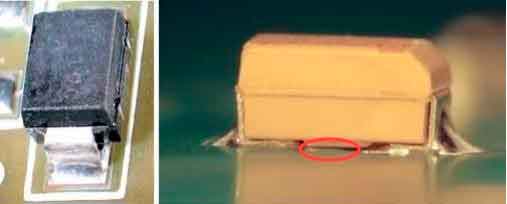
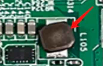
Real Case of Small Pad Causing Component Misalignment
Material Pad Size Doesn’t Match PCB Packaging Size
Problem Description: During SMT production, after reflow soldering, it was found that an inductor had shifted position. Upon investigation, it was discovered that the material pad size (3.31mm) did not match the PCB pad size (2.51.6mm), causing the material to twist after soldering.
Impact: The mismatch led to poor electrical connectivity, affecting the product’s performance. In severe cases, it resulted in the product failing to start.
Further Risk: If it is not possible to procure components with matching pad sizes that also meet the required inductance and current tolerance for the circuit, there is a risk of needing to modify the PCB design.
Chip Standard Package Pad Inspection
For chip standard package soldering reliability checks, three key aspects should be considered:
- Pad Length
- Pad Width
- Pad-to-Pad Spacing
These three factors are essential for ensuring that the chip can be properly mounted and soldered during the SMT process.