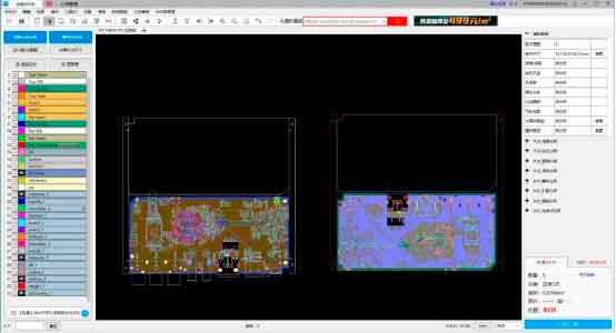
For PCB nesting, engineers are familiar with the basic rules, such as spaced or non-spaced nesting, using V-CUT or stamp holes for connections, adding process edges, positioning holes, and mark points. However, PCB come in various shapes, and simply following these basic rules is not enough. It is crucial to understand the production process in detail to ensure proper nesting, which will help avoid issues that may render the PCB unproducible or result in production scrap. The following examples highlight different PCB shape nesting cases for educational purposes.
CNC + V-CUT Nesting
Using Milling + V-CUT Nesting Method:
In this case, the nesting is done without spacing on the top, bottom, left, and right edges. If the PCB’s outer shape has irregular notches, non-spaced nesting becomes impractical. This is because small notches, which are smaller than the milling tool’s radius, cannot be milled properly, and burrs might form after milling. To avoid this, leave a 2mm spacing on the top and bottom, and ensure that no V-CUT is placed where there are notches. This way, the milling tool can avoid creating burrs, as shown in the images.
L-Shaped PCB Nesting:
For L-shaped PCBs, a turned-back nesting method is employed to save material. However, when the V-CUT lines are not aligned horizontally, it becomes impossible to use V-CUT for shaping. If V-CUT is skipped, the cost would increase significantly. The solution here is to leave 2mm spacing on the left and right edges to ensure proper V-CUT shaping, as shown in the diagram.
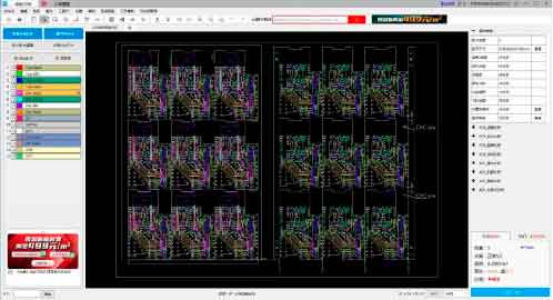
(pic-CNC + V-CUT-1)

Removing Burrs from the Edge of the PCB
V-CUT Bridging Nesting Method:
When using V-CUT bridging for nesting, if the outer shape lines are not aligned, sharp corners can occur, and the milling tool cannot reach those areas. A common solution is to add holes to drill the sharp corners. However, this approach is not ideal, as it may leave numerous burrs. Instead, a more practical method is to use V-CUT bridging for nesting, with added process edges. This way, even the smallest sharp corners can be milled properly without leaving burrs.

Irregularly Shaped PCB:
Irregularly shaped PCB cannot be nested using V-CUT, as doing so will result in sharp corners where the milling tool cannot reach, leaving burrs. For such irregular shapes, the stamp hole connection method should be used.

Half-Hole Board Nesting Methods
Half-Hole Position:
For half-hole boards, V-CUT cannot be used because it would cut through the copper in the half-holes, rendering them electrically non-functional. Instead, special processing should be applied to these half-hole positions, ensuring there is enough clearance for the milling tool to avoid damaging the copper, as shown in the image.

Half-Hole Boards with External Connections:
When nesting half-hole boards, especially when half-holes are located on the edges, it’s important to leave spacing for the milling tool. A turned-back nesting method is recommended for three-edge half-hole boards. This method places the milling-required areas together, leaving the areas without milling on the outside to simplify the connection. As shown in the diagram, non-spaced nesting would make the board unshapable.

Four-Sided Half-Hole Boards:
For four-sided half-hole boards, it is essential to leave sufficient clearance for milling. The corners should be connected using stamp holes to avoid board breakage due to small connecting areas. If the connection area is too small, you may consider not using stamp holes and directly connecting the board corners.

Considering Components at the Edge of the Board
Edge Components:
If components extend beyond the edges of the PCB, non-spaced nesting should not be used, as the components will interfere with others when nested. When designing boards with components extending beyond the edge, process edges must be added with cutouts to allow the components to be placed and soldered correctly.

Components Exceeding the Board Edge:
When nesting boards with components exceeding the edge, the turned-back nesting method should be used, with the extended components facing outward. This ensures that the assembly can take place without interference. If components are facing inward, they will collide with components on other boards, preventing assembly, as shown in the images.
Stamp Hole Bridging Nesting
Irregular and Round-Shaped PCB:
- Irregularly shaped or round boards must use stamp hole bridging for nesting, as V-CUT cannot be used on such shapes. For round boards, non-spaced V-CUT nesting may lead to small connection areas, which can cause the board to break easily. After production, the edges may also have burrs. When using stamp hole connections, it’s important to ensure the proper placement and spacing of the stamp holes. If the holes are placed too far apart, the board may break, and if the holes are too close, the connections may be insufficient and cause breakage.


Stamp Hole + V-CUT
Combination of V-CUT and Stamp Hole Nesting:
- For boards with irregular outer shapes, a combination of V-CUT and stamp hole connections may be used for nesting. However, the excess milling areas can cause the board to break. To prevent this, stamp holes should be added at the connection points to provide additional support and avoid board breakage.
(pic-Stamp Hole + V-CUT)