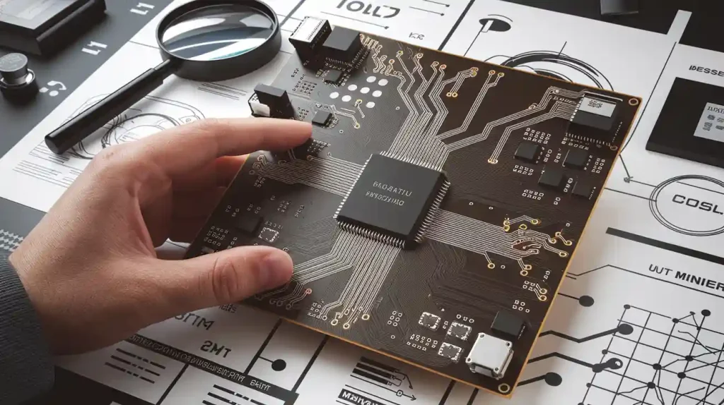
You face special problems when working with rf pcb. Strict rf layout rules help you get the best performance in any rf pcb design. RF signals act differently from normal signals. If you do not follow these rf layout rules, you might lose signal quality and trust. Careful design choices and following clear rules make your rf circuits steady and work well. This guide gives you the knowledge to solve every rf problem with confidence.
Key Takeaways
Make sure your traces have the right impedance. This keeps RF signals strong and stops signal loss. Use short and straight traces. Use solid ground planes to lower noise and keep signals clear. Pick PCB materials with a low dielectric constant and loss tangent. This helps high-frequency signals work better. Plan your PCB stackup with good layer order and grounding. This helps control interference. Keep analog, digital, and RF signals apart. Use shielding if you need to block noise.
RF PCB Design Basics
Key Principles
When you work with rf pcb layout, you need to use special rules. High-frequency signals can act in ways you do not expect. These signals can get weak or pick up noise if you do not follow the right pcb design guidelines. You have to keep signal integrity strong in every rf pcb design. This means your signals should stay clear as they move across the pcb.
Tip: Plan your rf pcb layout before you begin. Good planning helps you stop problems before they start.
Here are some important rules for every rf pcb layout:
Impedance Matching:
You need to match the impedance of your traces to the source and load. This keeps reflections low and signal integrity high. If you do not match impedance, your high-frequency signals can bounce back and cause mistakes.Short and Direct Traces:
Make your traces short and straight. Long or twisted traces can act like antennas. They can pick up signals you do not want and hurt your rf circuit design.Solid Ground Planes:
Put a solid ground plane under your high-frequency rf section. This gives your signals a clear path to return. It also helps lower noise and keeps your pcb layout steady.Minimize Crosstalk:
Keep traces far apart when you can. If traces are close, signals can jump from one to another. This crosstalk can mess up your signal integrity.Shielding and Isolation:
Keep your rf areas away from digital or power circuits. Use shielding if you need it. This keeps your rf signals clean and blocks outside noise.
Principle | Why It Matters in RF PCB Layout |
|---|---|
Impedance Matching | Keeps signal reflections low |
Short Traces | Reduces signal loss and interference |
Solid Ground Planes | Improves signal return and stability |
Minimize Crosstalk | Protects signal integrity |
Shielding/Isolation | Blocks outside noise and interference |
You should always check your rf pcb layout with these rules. Careful design choices help you avoid common mistakes in rf circuit design.
RF vs. Standard PCB
You may wonder how rf pcb design is different from standard pcb design. The answer is about how high-frequency signals act. In standard pcb layout, you can skip some small details. In rf pcb layout, every detail is important.
High-Frequency Effects:
High-frequency signals can leak energy into the air. They can also pick up noise from other parts of the pcb. You must control these effects with careful rf pcb layout.Impedance Control:
In standard pcb design, you may not worry about impedance. In rf pcb design, you must control impedance for every trace. This keeps your signal integrity strong.Signal Integrity:
You need to protect your signals from loss, noise, and distortion. High-frequency signals are more sensitive to these problems. You must use strict pcb design guidelines to keep your signals clean.PCB Stackup:
You often use special stackups in rf pcb. You may add extra ground layers or use special materials. This helps you control impedance and reduce interference.
Note: Always treat your high-frequency rf section with extra care. Small mistakes can cause big problems.
Here is a quick comparison:
Feature | Standard PCB | RF PCB (High-Frequency) |
|---|---|---|
Signal Frequency | Low to moderate | High-frequency |
Impedance Matching | Not always needed | Always needed |
Signal Integrity | Less critical | Very critical |
Layout Guidelines | Basic | Strict and detailed |
Material Selection | Standard FR-4 | Special low-loss materials |
You must follow strict pcb design guidelines for every rf pcb layout. This keeps your high-frequency signals strong and your rf pcb working well. When you use these guidelines, you build reliable and efficient rf circuits.
Material Selection
Dielectric Properties
When you make a high-frequency pcb, you need to look at the dielectric properties of the pcb substrate material. The dielectric constant (Dk) and loss tangent (Df) are two key numbers. These numbers show how signals move and how much energy they lose. If the pcb substrate material has a high Dk, signals move slower. If the Df is high, signals lose more energy as heat.
High-frequency signals work best with a pcb substrate material that has a low Dk and a low Df. This keeps signals moving fast and strong. If you do not pay attention to these properties, your high-frequency signals can get weak or mixed up. You want your pcb to help signals move clearly and reliably.
Tip: Always look at the datasheet for dielectric properties before you choose a pcb substrate material for high-frequency designs.
Common Materials
You can pick from many pcb substrate materials for high-frequency uses. Each material has good and bad points. Here are some common choices:
FR-4: This material is used in many standard pcb designs. It is good for low-frequency circuits, but not for high-frequency.
Rogers (RO4000, RO3000): This pcb substrate material has low loss and steady dielectric properties. It is often used for high-frequency circuits.
PTFE (Teflon): This material has very low loss and a steady Dk. It is great for very high-frequency pcb designs.
Ceramic-filled materials: These materials give better heat control and low loss at high-frequency.
Material Type | Dielectric Constant (Dk) | Loss Tangent (Df) | High-Frequency Suitability |
|---|---|---|---|
FR-4 | 4.2 – 4.7 | 0.02 | Low |
Rogers RO4000 | 3.38 | 0.0027 | High |
PTFE (Teflon) | 2.1 | 0.0002 | Very High |
Ceramic-filled | 3.0 – 10 | 0.001 – 0.005 | High |
When you pick a pcb substrate material, think about your high-frequency needs, the cost, and how easy it is to make the pcb. Always choose a material that fits your signal needs.
RF PCB Stackup
Layer Arrangement
You need to plan your pcb stackup before you start your design. The way you arrange the layers in your pcb affects how signals move and how much noise you get. A good stackup helps you control impedance and reduce interference. You can use a simple two-layer pcb, but most rf designs work better with four or more layers.
A common stackup for rf pcb uses these layers:
Top layer: Signal
Second layer: Ground plane
Third layer: Power or signal
Bottom layer: Ground plane or signal
You should place your signal layers close to a ground plane. This keeps the impedance steady and helps your signals stay clean. If you use more layers, you can add extra ground planes for even better performance.
Tip: Always keep your signal traces as close as possible to a ground plane. This helps you avoid unwanted noise.
Signal and Ground Layers
The ground plane is one of the most important parts of your rf pcb. You need a solid ground plane under your signal layers. This gives your signals a clear return path and lowers the risk of interference. If you break up the ground plane, you can cause signal problems.
You should connect your ground plane with many vias. This keeps the ground plane strong and helps stop noise from spreading. You can use a table to see how a good stackup looks:
Layer Number | Layer Type | Notes |
|---|---|---|
1 | Signal | Place close to ground plane |
2 | Ground plane | Solid, no breaks |
3 | Power/Signal | Keep away from rf signals |
4 | Ground plane | Extra return path |
You should always check your pcb stackup before you build your board. A strong ground plane and smart layer arrangement help you get the best rf performance.
Trace Design
Controlled Impedance
You must control impedance in every rf pcb layout. Controlled impedance keeps your rf signals strong and clear. If you do not match the impedance, your rf traces can cause reflections. These reflections hurt signal quality. You should use the right width and spacing for each rf trace. The pcb material and stackup also change the impedance. Always check your rf pcb layout with a calculator or simulation tool.
Tip: Use the same width for all rf traces that carry the same type of rf signal. This helps you keep impedance steady across your rf pcb layout.
Microstrip and Stripline
You will often use microstrip or stripline structures in rf pcb layout design. Microstrip traces sit on the top layer of the pcb with a ground plane below. Stripline traces run between two ground planes inside the pcb. Each type has its own use in rf pcb trace design.
Structure | Location on PCB | Shielding Level | Typical Use |
|---|---|---|---|
Microstrip | Top layer | Medium | Simple rf routing |
Stripline | Inner layer | High | Sensitive rf transmission lines |
Microstrip is easy to make and inspect. Stripline gives better shielding for your rf traces. You should pick the right type for your rf pcb layout.
Routing Guidelines
You need to follow special rules for rf routing. Keep your rf traces as short and straight as possible. Avoid sharp corners. Use gentle bends instead. This stops signal loss and keeps your rf signals clean. Do not cross rf traces over splits in the ground plane. This can cause noise and signal problems.
Place rf traces away from noisy digital lines.
Use via stitching to connect ground planes near rf transmission lines.
Keep the spacing between rf traces wide to lower crosstalk.
Remember: Careful rf pcb layout and smart rf routing help you avoid signal loss and interference.
You should always review your rf pcb layout before you finish. Good rf pcb trace design makes your rf circuits work better and last longer.
Impedance Design
Theoretical Foundations
Impedance is very important in rf pcb design. You must control impedance to keep signals clear. Impedance is like resistance for signals moving on a trace. In rf, signals travel very fast. If impedance changes, signals can bounce back. These bounces make noise and weaken your rf signals. You should match the impedance of traces to the source and load. This keeps your rf circuit design steady and stops signal loss.
Key Factors Affecting Impedance
Many things can change impedance in your rf pcb. You need to watch these things when you design:
Trace width: Wider traces lower impedance. Narrow traces raise impedance.
Dielectric thickness: The space from trace to ground plane changes impedance.
Dielectric constant: The pcb material type changes how signals move.
Copper thickness: Thicker copper changes impedance in your rf traces.
PCB stackup: How you arrange layers in your rf pcb changes impedance.
Always check these things before you finish your rf design. Small changes can really affect signal quality.
Impedance Calculation Methods
You can use different ways to find the right impedance for rf traces. Many engineers use online calculators or special software. You can also use formulas for microstrip or stripline traces. Here is a simple formula for microstrip impedance:
Z = (87 / sqrt(Dk + 1.41)) * ln(5.98 * H / (0.8 * W + T))
Where:
Z = impedance (ohms)
Dk = dielectric constant
H = height from trace to ground plane
W = trace width
T = trace thickness
You should always check your answer with a tool or simulation. This helps you keep signals strong in your rf pcb.
Practical Design Workflow
You can follow these steps to control impedance in your rf pcb design:
Choose your pcb material and stackup.
Set your target impedance for each rf trace.
Use a calculator or tool to find the right trace width.
Draw your rf traces with the right width and space.
Check your layout with a simulation tool.
Review your design to make sure you meet all rf and signal needs.
Careful planning helps you avoid problems and keeps your rf signals strong.
Grounding Techniques
Ground Planes
You need a strong grounding plan for every rf design. A solid ground plane gives your rf signals a clear path. This helps you lower noise and keep your signals clean. Place a ground plane under your rf traces. This makes your grounding better and helps with signal return. If you break up the ground plane, you can cause problems in your rf circuit. Always keep the ground plane as large and unbroken as possible.
Tip: Use a full ground plane under your rf section. This simple grounding step can stop many signal issues.
A good grounding strategy uses a single ground plane for all rf parts. This keeps your rf signals steady and helps you avoid interference.
Via Stitching
Via stitching connects different ground layers in your rf pcb. You place many small vias along the edge of your rf ground plane. These vias link the top and bottom ground planes. This grounding method stops noise from spreading. You also use via stitching to keep your rf signals inside the right area.
Place vias close together for better grounding.
Use via stitching around rf traces and near sensitive parts.
A table can help you see where to use via stitching:
Area | Via Stitching Needed? |
|---|---|
RF trace edges | Yes |
Shielded sections | Yes |
Digital sections | Sometimes |
Return Paths
You must give your rf signals a clear return path. Good grounding makes this easy. If the return path is broken, your rf signals can pick up noise. Always route your rf traces over a solid ground plane. This keeps the return path short and direct. If you split the ground plane, you make the return path longer. This can hurt your rf performance.
Remember: Good grounding gives your rf signals a safe way back. This keeps your circuit strong and reliable.
You should always check your grounding before you finish your rf pcb. A strong grounding plan helps every rf design work better.
Power and Decoupling
Power Routing
You must plan power routing carefully in RF PCB design. High-frequency circuits need power that is clean and steady. If you do not route power lines well, noise can happen. This noise can make your signal quality worse. Use wide power traces or planes for better results. Wide traces lower resistance and keep voltage steady. Power planes also help stop noise from spreading.
Tip: Keep power traces away from sensitive RF signal lines. This helps stop unwanted coupling and interference.
Here are steps for better power routing:
Try to use a dedicated power plane.
Keep power traces short and direct.
Do not use sharp corners in power lines.
Place power and ground planes close together in the stackup.
This table shows good and bad power routing:
Power Routing Practice | Effect on RF PCB |
|---|---|
Wide traces/planes | Lower noise, stable power |
Long, thin traces | Higher noise, voltage drop |
Close to ground plane | Better noise control |
Decoupling Placement
Decoupling capacitors help block noise from the power supply. Put these capacitors close to each RF chip or part. If you put them far away, they cannot block high-frequency noise well. Use capacitors with low equivalent series resistance (ESR) for best results.
Place a small-value capacitor, like 0.01 µF, right next to each RF IC power pin. Add a bigger capacitor, like 1 µF, nearby for low-frequency filtering.
Use this checklist for decoupling placement:
Put capacitors as close as you can to power pins.
Use more than one value for wide frequency coverage.
Connect capacitors to the ground plane with short traces.
Good decoupling keeps your RF signals clean and your circuit steady. Always check your layout to make sure you have enough decoupling near every RF part.
Isolation and Shielding
Signal Separation
You need to keep different signals apart on your RF PCB. When you separate signals, you stop unwanted noise from moving between them. Place analog and digital signals on different areas of your board. This helps each signal stay clean and strong. You should also route high-frequency lines away from low-frequency lines. If you cross signal paths, do it at a right angle. This reduces the chance of interference.
Tip: Use clear labels and zones for each signal type. This makes your layout easier to check and keeps signals safe.
A simple table can help you plan signal separation:
Signal Type | Placement Advice |
|---|---|
Analog | Far from digital signals |
Digital | Away from RF sections |
RF | Isolated with ground plane |
You can use ground planes as barriers between signal types. This adds another layer of protection.
EMI Reduction
You must control emi to keep your RF PCB working well. emi stands for electromagnetic interference. It can cause your signals to lose quality or even fail. Shielding is a strong way to block emi. You can use metal shields over sensitive parts. These shields stop outside noise from reaching your circuits.
You should also use via stitching around shielded areas. This keeps the shield connected to the ground and blocks more emi. Short traces and solid ground planes help lower emi as well.
Place shields over RF chips and antennas.
Use ground fills between signal lines.
Keep high-speed signals away from board edges.
Remember: Good shielding and smart layout choices protect your board from emi and keep your signals clear.
Layout Tips for RF PCB
Component Placement
You need to plan your pcb layout before you start placing parts. Good placement helps your design work well. Put antennas at the edge of your board. This keeps them away from noise and lets them send and receive signals better. Place transmitters and receivers close to the antenna. Short traces help you follow pcb design guidelines and keep your signals strong.
Switches and other high-frequency parts should stay near the signal path. If you work with mixed-signal pcb, keep analog and digital parts apart. This stops noise from moving between them. Use a ground plane to separate these zones. You can use a table to help plan your placement:
Component | Placement Tip |
|---|---|
Antenna | Edge of board, clear space |
Transmitter | Close to antenna |
Receiver | Close to antenna |
Switch | Near signal path |
Minimizing Parasitics
Parasitics are unwanted effects that can hurt your pcb layout. You need to keep traces short and direct. Long traces act like antennas and pick up noise. Follow pcb design guidelines to avoid sharp corners. Use smooth bends instead. Place decoupling capacitors close to power pins. This helps your design block noise.
If you work with mixed-signal circuits, keep analog and digital traces apart. Do not cross them if you can help it. If you must cross, do it at a right angle. This lowers the chance of noise moving between signals.
Tip: Always check your pcb layout for extra copper or unused pads. Remove them to lower parasitics.
Manufacturing Factors
You must think about manufacturing when you finish your pcb layout. Use standard trace widths and spacing that your factory can make. Follow pcb design guidelines for hole sizes and pad shapes. If you use mixed-signal pcb, tell your manufacturer about special needs. This helps them make your design right.
Check that your board can be made without errors. Avoid very small gaps or thin traces. These can break during production. Good pcb layout helps you get a board that works the first time.
Remember: Careful planning and following pcb design guidelines make your design easier to build and test.
You now have an easy guide for good rf pcb design. Follow these steps to make every rf pcb work better. Plan your design before you start. Pick the right materials for your board. Lay out your parts with care. Use strong grounding and keep signals apart. This helps your board work well. Check your work to find mistakes early. This guide helps you do your best. If your rf pcb is hard, ask an expert or look for more help.
FAQ
What is the most important rule in RF PCB design?
You must match the impedance of your traces. This keeps your signals strong and clear. Impedance matching stops reflections and signal loss. Always check your trace width and material to get the right impedance.
How do you reduce noise in an RF PCB?
You can use a solid ground plane under your RF traces. Place decoupling capacitors close to power pins. Keep digital and analog signals apart. Short traces help lower noise, too.
Which material works best for high-frequency RF PCBs?
PTFE (Teflon) gives you very low loss and stable signals at high frequencies. Rogers materials also work well. FR-4 is not good for high-frequency designs.
Material | High-Frequency Use |
|---|---|
PTFE | Excellent |
Rogers | Very Good |
FR-4 | Poor |
Why should you keep RF traces short and straight?
Short, straight traces keep your signals strong. Long or bent traces can act like antennas. They pick up noise and lose signal quality. Always plan your layout for the shortest path.
Do you need shielding for every RF circuit?
Not every RF circuit needs shielding. You should use shielding if you see a lot of noise or interference. Metal shields and ground fills help protect sensitive parts. Always test your board to decide if shielding helps.