You need expert tips to design mobile PCB systems for new smartphones. The printed circuit board helps all parts connect and work together in your device. You should think about where to put parts early. Focus on how traces are routed. Be careful when you use vias. The table below shows the most common tips from recent technical articles:
Tip | Description |
|---|---|
Early Component Placement | Make sure the layout is good. This helps avoid parts bumping into each other. It also makes assembly easier. |
Trace Routing and Signal Integrity | Keep trace width and spacing right. This helps signals stay strong and clear. |
Via Management | Do not use too many vias. Pick the right size to save money. |
Testing and Debugging | Add test points. This makes debugging and testing easier. |
Keep learning about new materials and ways to make PCBs. You can make mobile phone PCBs work better and last longer by using these design tips.
Key Takeaways
Plan where you put parts early. This helps you avoid errors. It also makes building easier.
Keep trace width and spacing correct. This helps signals stay strong and clear.
Use fewer vias when you can. Pick the right size for them. This saves money and makes the board work better.
Add test points to your design. This makes debugging and testing easier.
Learn about new materials and technologies. This helps your PCB work better and last longer.
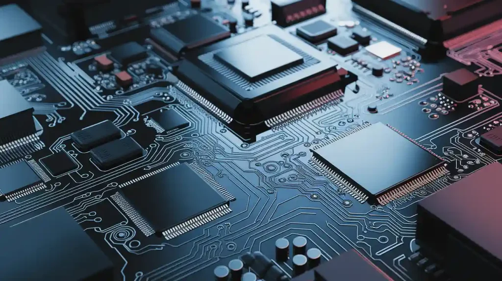
Mobile PCB Design Fundamentals
Types of Printed Circuit Boards
Smartphones use different types of printed circuit boards. The most used type is the multilayer pcb. These boards have many layers stacked on top of each other. This lets you fit more circuits and parts in less space. Multilayer boards help signals move quickly and stop interference. They also make smartphones lighter and smaller. These boards are strong and last a long time.
Multilayer pcb lets you fit more circuits in one place.
It helps signals move fast and clear.
It makes mobile phone pcb designs smaller and lighter.
It makes the board stronger and tougher.
Key Components and Functions
It is important to know the main parts of a mobile pcb. Each part has its own job. Chips handle data and run apps. Capacitors hold and give out energy. Resistors slow down the flow of electricity. Connectors join the board to other phone parts. Traces are thin lines that send signals between parts. Vias let signals move from one layer to another in a multilayer board.
Tip: If you know what each part does, you can plan your pcb design better and make fewer mistakes.
Essential PCB Design Steps
You should follow easy steps when you design a mobile pcb. Here are the main steps:
Place parts smartly to save space.
Keep signals strong by planning well.
Control heat by thinking about how it spreads.
Test your design with careful checks to make sure it works.
If you learn these basics, you will have a good start for your mobile phone pcb project. Good planning and knowing the basics help you make better printed circuit board designs for new smartphones.
Mobile PCB Challenges and Solutions
Miniaturization and Density
You face big challenges when you make mobile PCBs smaller and more packed. As you shrink the printed circuit board, you must fit more parts into less space. This makes it harder to keep everything working well. The table below shows the main problems you will see:
Challenge | Description |
|---|---|
Signal Integrity and EMI | You must control crosstalk and impedance. More parts close together can cause signals to mix and create noise. |
Thermal Management | Small boards get hot fast. You need good cooling or parts may fail. |
Manufacturing Complexity | You need precise placement and soldering. Mistakes can happen more easily when everything is tiny. |
To solve these problems, you can use new technologies and smart design tricks. Here are some ways you can make your mobile phone pcb more dense and reliable:
HDI technology uses thin copper lines and laser microvias. You can route more connections in a small space.
You can use high-performance thin materials. These help you fit advanced features into compact devices.
Buried resistors go inside the layers of the multilayer pcb. You save space on the surface and keep your design tight.
These resistors also help you keep good electrical performance while shrinking the board.
Tip: When you plan your pcb layout, always check for enough space between traces. This helps you avoid signal problems and makes your board easier to build.
High-Frequency Signal Integrity
You must protect signals when you design for high-frequency use. Fast signals can lose strength or get mixed up if you do not plan well. The core thickness and substrate properties matter a lot. If the substrate has a high dielectric constant, signals slow down. This can cause timing problems. If the core is too thick, the impedance changes. For example, a core thickness of 0.2 mm may give you 50 ohms, but 0.4 mm can raise it to 75 ohms. If the impedance does not match, signals bounce back and create noise. Thicker cores also absorb more energy, which means more signal loss.
You can use these techniques to keep your high-frequency pcb design strong:
Grounding and Shielding: You add grounding layers and shields. These keep signals from mixing and cut down on noise.
Impedance Matching: You match the trace impedance to the parts. This stops signal reflections and keeps signals clear.
Differential Signaling: You use two opposite signals. This keeps transmission steady and reduces noise, which is important for high-speed devices.
Note: Always check your interconnect paths and test for signal loss. Good planning helps you keep your mobile pcb working fast and reliable.
Thermal Management
Heat is a big problem in small and powerful devices. You must keep your mobile pcb cool or parts may stop working. The table below shows the most common thermal problems:
Challenge | Description |
|---|---|
Compact Size | Phones are thin. You do not have much room for big cooling parts. |
High Power Density | Chips make more heat in a small area. This can cause hot spots. |
Cost Constraints | Fancy cooling materials cost a lot. You must balance price and performance. |
User Expectations | People want fast phones that do not get hot or drain the battery. |
You can use these solutions to manage heat in your pcb design:
Solution Type | Description |
|---|---|
Thermal Interface Materials | These help heat move from parts to cooling areas. |
Thermal Gap Fillers | These fill spaces between hot parts and coolers, keeping heat moving well. |
Thermal Insulators | These block heat from reaching sensitive parts. |
Heat Sinks | These pull heat away from parts and spread it into the air. |
Heat Spreaders | These move heat over a bigger area, making it easier to cool. |
Heat Pipes | These move heat quickly from one place to another, keeping the board cool. |
Tip: When you design your multilayer pcb, always plan for heat flow. Place hot parts near cooling solutions and use good materials to keep your board safe.
PCB Materials and Layer Stackup

Advanced Substrate Choices
You have to pick the best materials for your printed circuit board. The substrate is the bottom layer that holds all the parts. The type of substrate you pick changes how your mobile pcb works. This is very important for fast and powerful smartphones. Here are some advanced substrate choices you should know about:
High-frequency laminates keep signals clear. They have a low dielectric constant and loss tangent. You can use them for RF and microwave circuits.
Polyimide substrates are good for heat and can bend. They work well in tough places or when you need flex pcb materials.
Metal-core substrates have a metal base. This helps move heat away from hot parts. You need this for high-power uses.
Ceramic substrates move heat well and block electricity. You can use them in high-power and high-temperature designs.
The substrate you pick also changes how fast and clear signals move. A lower dielectric constant lets signals go faster. PTFE is a good example. It works well in 5G devices because it has a low dielectric constant. Polyimide and PTFE help keep signal loss low, which is important for fast circuits. Substrates like FR-4 block electricity well and are used in many designs.
Tip: Always pick a substrate that fits your device’s needs. This helps your device work better and last longer.
Optimizing Stackup for Performance
You need to plan your pcb layer stackup with care. The stackup is the order of layers in your multilayer pcb. A good stackup helps your device run fast and stay cool. Here are some best ways to design your stackup:
Put ground planes next to signal layers. This cuts down on noise and crosstalk.
Place power planes in the middle. This spreads power and lowers interference.
Use controlled impedance. Make sure your signal traces are the right width and spacing. For example, 50 ohms is common for RF signals.
Use microvias and blind vias. These save space and keep signals strong in tight designs.
Pick dielectric materials with the right thickness and low dielectric constant. Values around 3.5 to 4.5 work well for mobile phone PCBs.
How you put copper and insulating layers together changes how heat and signals move. Thicker copper layers help spread heat and keep your device steady. A smart stackup also makes power flow better and keeps your device from getting too hot.
Note: A good stackup can help your smartphone last longer and work better.
Cost and Reliability Factors
You need to think about cost and reliability when you pick materials and stackup for your pcb. Fancy materials can make your device work better, but they cost more. Here are some things that change the cost:
If you use advanced materials, you may pay 10-20% more than normal ones.
Meeting rules and keeping records can add 5-15% to your costs.
Testing and certification can cost $500 to $5,000 for each batch.
Upgrading your machines for new materials can cost $10,000 to $50,000.
You also want your device to last and work well. The table below shows how different materials help with reliability:
Material Type | Key Benefits |
|---|---|
FR4 | Cheap, good electrical properties, good for basic designs. |
Polyimide | Great for flexible uses, stops cracking in bendy designs. |
PTFE (Teflon) | Low dielectric constant, little signal loss, good for high-frequency use. |
Ceramic | Great for high-power uses, moves heat away well. |
If you use the right materials, your pcb design will be strong and reliable. Polyimide is good for flexible and bendy devices. PTFE is best for fast signals. Ceramic is good for devices that get hot. FR4 is a good pick for simple and cheap designs.
Tip: Always balance cost, how well it works, and reliability. This helps you make better smartphones for the future.
Rigid-Flex and Flexible Mobile Phone PCBs
Benefits for Modern Smartphones
More smartphones use rigid-flex and flexible printed circuit boards now. These boards help make phones smaller and add more features. You can bend and fold the board to save space. This makes your phone thinner and lighter. The table below shows how these boards help new devices:
Benefit | Application | Impact |
|---|---|---|
Space Efficiency | Smartphones, wearables | Makes the device smaller |
Improved Durability | Multi-function mobile devices | Stops damage from bending and flexing |
Enhanced Performance | High-performance consumer electronics | Keeps signals strong and saves power |
Rigid-flex boards last longer and work better. They also help you keep up with new pcb trends in 2026.
Design Considerations for Flexibility
When you design flexible printed circuit boards, think about how they will bend. Plan the right bend radius so the board does not break. Use narrow traces and spaces to keep signals clear. Put parts away from places that will bend. Pick materials that can bend and handle tough use. Think about heat, water, and chemicals that could hurt your board.
Bend radius keeps your board safe.
Trace and space width keeps signals clear.
Component placement stops problems when bending.
Material choice helps your board bend and last.
Environmental checks protect your board in tough places.
Tip: Always test your printed circuit boards to make sure they bend well before you finish your design.
Material Selection for Bend Life
You need good materials so your mobile pcb can bend many times. The table below shows which materials are best for flexible printed circuit boards:
Material Type | Key Properties | Effectiveness in Bend Life |
|---|---|---|
Rolled Annealed Copper | Bends many times without breaking, good for moving designs | Lasts longer because it does not crack |
Polyimide | Very bendy, handles heat, bends in tight spaces | Works well for both still and moving uses |
Adhesive-less Laminates | Thin layers, less chance of cracking | Makes boards bend better and last longer |
Coverlay | Protects from damage, stays bendy | Best for moving boards because it is tough |
Rolled annealed copper and polyimide are best for flexible boards. These materials help your multilayer pcb stay strong and bendy. Adhesive-less laminates and coverlay also make your board last longer in new pcb designs.
Note: Picking good materials helps your printed circuit boards last longer and work better in small and bendy devices.
AI and Automation in PCB Design
AI-Driven Layout Tools
You can use ai-driven layout tools to help design your pcb faster. These tools do many jobs for you, like putting parts in place and checking for mistakes. This means you do not have to do the same work over and over. You can spend more time on hard problems. Ai finds spacing and clearance problems early. It keeps looking for errors as you work. This way, you do not have to fix big mistakes at the end. Ai also helps you pick the best spots for parts. This makes your board better at handling heat and power.
Tip: Ai-driven layout software helps you finish designs faster, make fewer mistakes, and get better boards. You can spend more time on the most important parts of your pcb.
Automated Routing and Testing
Automated routing and testing tools make your pcb more exact. These tools handle trace routing and via placement for you. You get feedback right away about your design limits. Ai can find and fix signal problems before they happen. This helps your board work well at high speeds. You save time and get better boards.
Evidence Description | Key Benefits |
|---|---|
AI tools do jobs like trace routing and via placement. | Engineers have more time to solve problems. |
AI checks design limits and gives feedback right away. | This makes designs more correct and efficient. |
AI finds and fixes signal problems before they start. | Your board works well at high speeds. |
Speeding Up Prototyping
You can make prototypes faster by using quick services and new tech. Quick-turn services let you get simple boards in one or two days. Fast prototyping lets you test many ideas quickly. You find problems early and save money, sometimes up to 40%. You can use 3D printing and other new ways to make prototypes even faster. Testing again and again helps you make your design better and get the best board.
Use fast prototyping services to get boards quickly.
Test and fix your design with each new try.
Try new tech to make prototyping even faster.
Note: Trying ideas quickly and using new tools helps you make better smartphone pcbs in less time.
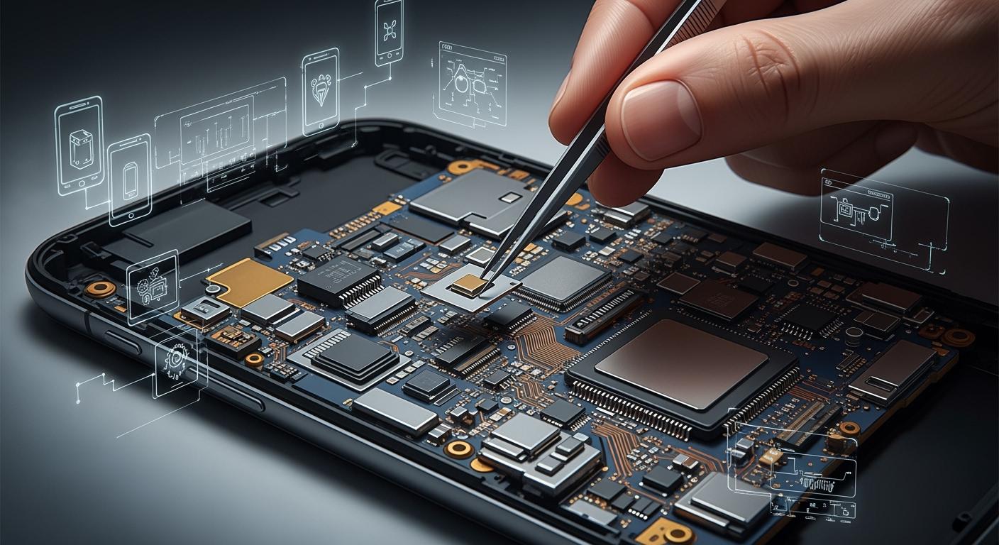
Mobile Phone PCB Manufacturing and Quality
Design for Manufacturability
You should think about manufacturability at the start of your pcb design. This helps you stop problems like via damage or electrical shorts. There are some important steps you can follow to make sure making your pcb is easy:
Check copper spacing and drill sizes so you do not get shorts.
Make sure annular rings and thermal relief patterns are correct.
Pick the right soldermask setup for your board.
Follow IPC-2221 and other rules to keep your board reliable.
Always talk with your manufacturer. Send your files for review and change things before you finish.
Tip: If you follow what your manufacturer says, you make fewer mistakes and your pcb will be better.
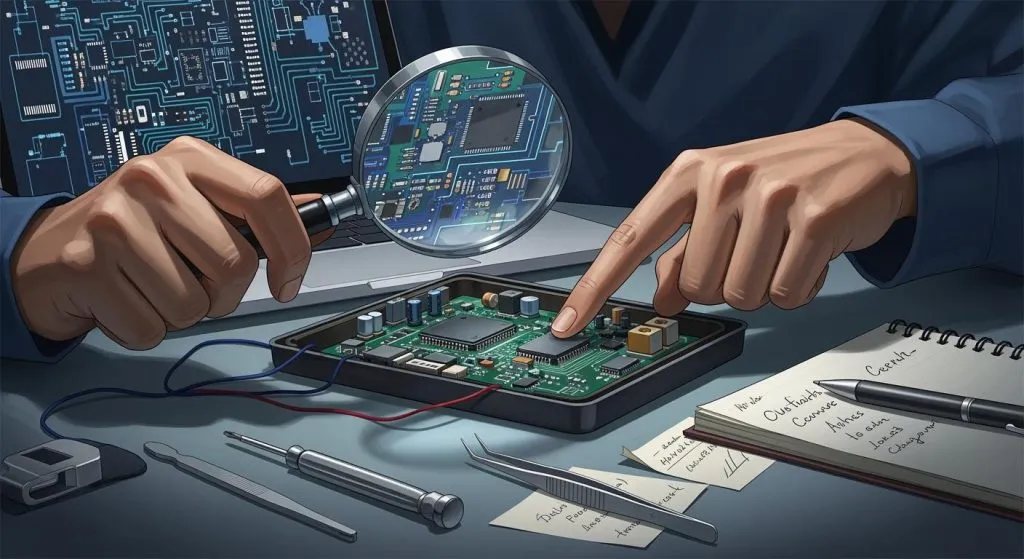
Inspection and Testing Methods
You need good inspection and testing to make sure your pcb works. Here are the best ways to check your board:
Method | Description |
|---|---|
X-ray Inspection | Finds hidden problems like holes in solder joints and cracks inside multilayer boards. |
In-Circuit Testing (ICT) | Checks if each part on the pcb works by measuring resistance, voltage, and signals. |
Automated Optical Inspection (AOI) | Uses cameras to look for defects on the surface and helps catch errors early in the process. |
Note: These methods help you find problems before your product goes to customers.
Supply Chain Strategies
You need smart supply chain plans to get the right parts for your pcb. Start with an Approved Vendor List so you get good parts. Work with trusted sellers and watch market trends. Build strong relationships with suppliers for better prices and more parts. Use tools to keep track of your inventory. Plan for backups so you do not depend on just one supplier. Just-in-Time plans help you keep less inventory and get new parts fast. Always check for quality and plan for parts that may not be made anymore. Long-term deals can help you keep prices and supply steady.
Tip: Good supply chain planning keeps your pcb making smooth and helps you avoid delays that cost money.
Sustainability in PCB Production
Eco-Friendly Materials
You can pick eco-friendly materials to help the earth. Many companies use tin, silver, or copper instead of lead now. Halogen-free laminates are used instead of old flame retardants. Recyclable substrates help make a circular economy work. The table below shows some common choices:
Traditional Material | Eco-Friendly Alternative |
|---|---|
Lead | Tin, Silver, Copper |
Halogenated Flame Retardants | Halogen-Free Laminates |
Recyclable Substrates | Supports Circular Economy |
You can use closed-loop water systems to clean water during making. Advanced filters help keep water clean too. Chemical recycling and machines that use green energy help lower pollution.
Designing for Recyclability
You can design your pcb so it is easier to recycle. Pick high-grade polyimide for flex boards so they last longer. Use lead-free and safe materials to lower harm when you throw away old devices. Try bio-based substrates to cut down your carbon footprint. Here are some ways to make recycling better:
Pick sustainable materials like halogen-free laminates and lead-free solder.
Make modular designs with clear space so repairs are easy.
Plan layouts to use less material and make less waste.
Design so you can take things apart and reuse them.
If you plan for long life and easy repair, you help keep devices out of landfills.
Meeting Global Standards
You must follow world rules to make your production green. Use eco-friendly materials and lead-free finishes. The WEEE directive says you must recycle and throw away electronic waste the right way. You need to handle dangerous chemicals like acids, heavy metals, and volatile organic compounds. Following these rules helps keep people and nature safe.
Tip: Always check new rules and use safe materials. This helps you make better devices and protect the earth.
Future Trends in Mobile PCB
6G and Advanced Connectivity
You will see big changes in smartphone technology as 6G networks arrive. 6G will give you faster speeds and lower delays than 5G. Your phone will connect to more devices at once. You will use new sensors and cameras that need strong signal paths. You must design your pcb to handle higher frequencies and more data. You will need better shielding and grounding to keep signals clear. You will also use new materials that help signals move faster.
Tip: Start learning about 6G standards now. You will be ready when new phones need advanced connectivity.
Innovations in Power Management
You will need smarter ways to save energy in future smartphones. New chips use less power but work faster. You will see batteries that charge quickly and last longer. You can use power-saving circuits that turn off parts of your phone when you do not use them. You will add sensors that watch battery health and temperature. You can use wireless charging and energy harvesting to keep your phone running. You will design your pcb to support these new power features.
Power Management Feature | Benefit |
|---|---|
Fast Charging | Less waiting time |
Energy Harvesting | Longer battery life |
Smart Sensors | Safer and cooler phones |
Evolving Manufacturing Techniques
You will use new ways to make mobile phone pcbs. You can use robots to place parts faster and with fewer mistakes. You will see 3D printing used for small parts and custom shapes. You can use laser drilling for tiny holes and fine lines. You will use better inspection tools to find problems early. You will also use eco-friendly methods to lower waste and save energy.
Robots help you build boards quickly.
3D printing lets you try new designs.
Laser drilling makes your board more precise.
Green methods protect the planet.
Note: Stay updated on new manufacturing techniques. You will make better phones and help the environment.
You can design better mobile PCBs by following expert tips. Place components early, route traces with care, and choose strong materials. Test your board often and use AI tools to speed up your work. Pick eco-friendly options and plan for recycling. Stay updated with new trends like 6G and flexible boards.
Remember: Master the basics and keep learning. You will build smarter, faster, and greener smartphones.
FAQ
What is the most important thing to remember when designing a mobile PCB?
You should always plan your layout before you start. Early planning helps you avoid mistakes and makes your board easier to build.
How do you keep a mobile PCB cool?
You can use heat spreaders, thermal pads, or special materials. Place hot parts near cooling areas. Test your design for hot spots.
Why do you need flexible PCBs in smartphones?
Flexible PCBs let you fit more parts in small spaces. You can bend them to connect different sections. This makes your phone thinner and lighter.
What tools help you design PCBs faster?
AI-driven layout software
Automated routing tools
Quick-turn prototyping services
These tools help you finish your design quickly and find errors early.
How can you make your PCB design eco-friendly?
Step | Benefit |
|---|---|
Safer for the planet | |
Pick recyclable materials | Less waste |
Design for repair | Longer device life |