Xenon Plasma Focused Ion Beam (PFIB) technology works faster than gallium-based Focused Ion Beam systems. It is also more efficient. Many labs that study broken semiconductors now like PFIB better. PFIB can work with big amounts and tricky shapes easily. The industry is clearly changing what it likes to use:
The Failure Analysis part is a big part of the Focused Ion Beam market.
Labs are switching from gallium ion sources to Xenon plasma sources.
Newer sources help with things like 3D NAND and packaging analysis.
These changes show that people want better and more trustworthy tools for checking semiconductors.
Key Takeaways
Xenon PFIB works faster and better than Ga-FIB. It is good for big jobs and hard materials. Using Single Crystal Sacrificial Masks with PFIB keeps surfaces safe. It also stops extra marks during testing. Engineers should pick PFIB for big samples and strong materials. Ga-FIB is best for small and careful work. Automation in PFIB helps labs finish work faster. It also helps people make fewer mistakes. This makes labs do more work. Standard rules help labs get the same results. This makes people trust semiconductor analysis more.
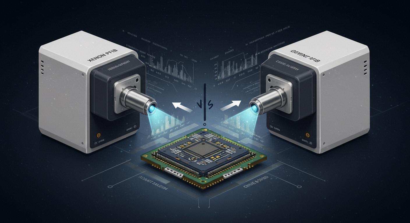
PFIB vs. Ga-FIB
Speed and Efficiency
Speed and efficiency are very important in semiconductor failure analysis. Xenon Plasma Focused Ion Beam (PFIB) technology mills faster than gallium-based systems. This is because Xenon PFIB has a higher ion current and sputtering rate. Labs can finish big jobs much quicker, which saves time and helps them do more work.
The table below shows the main differences in how they work:
Feature | Xenon PFIB | Ga-FIB |
|---|---|---|
Ion Current | Lower (nanoamps) | |
Sputtering Rate | Higher | Lower |
Efficiency in Milling | Higher for large areas | Moderate |
Efficiency in Material Removal | High efficiency at high currents | High efficiency but lower than Xe-FIB |
Many labs say Xenon Plasma Focused Ion Beam (PFIB) works better than Ga-FIB for big jobs. PFIB also does well with tiny patterns when using low currents. These upgrades help engineers finish hard tasks faster.
Sample Impact
Keeping the sample safe is very important during analysis. Ga-FIB systems have trouble with big or thick samples. They can only work with small amounts of material. Xenon PFIB systems can handle bigger samples and lower the chance of damage.
Tip: Xenon PFIB can get samples ready for 3D tomography, SEM, and TEM with less risk of mistakes.
The next table shows how Xenon PFIB fixes Ga-FIB problems:
Limitation of Ga-FIB | Advantage of Xenon PFIB |
|---|---|
Limited material volume handling | Can handle larger volumes of material |
Inefficient milling of challenging materials | |
Basic sample preparation capabilities | Enhanced sample preparation for 3D tomography, SEM, and TEM |
Engineers see fewer mistakes and better surfaces when using Xenon PFIB. This means the results are more trustworthy.
Material Compatibility
Material compatibility helps decide which tool to use. Ga-FIB works for many normal materials but has trouble with hard metals and tricky shapes. Xenon Plasma Focused Ion Beam (PFIB) technology can work with more types of materials, like tungsten, nickel, and steel. This makes PFIB a better choice for new semiconductor devices and packaging.
PFIB can mill big areas of aluminum alloys, which is needed for transmission electron microscopy (TEM) samples.
Ga-FIB does not work as well for these tough jobs.
Engineers who work with new devices like that PFIB works with more materials and is faster. This technology helps with the newest ways to make and check semiconductors.
Xenon Plasma Focused Ion Beam (PFIB) Technology
High Current Benefits
Xenon Plasma Focused Ion Beam (PFIB) technology is special because it uses much higher ion beam currents than gallium systems. This high current helps engineers take away material quickly. It makes sample preparation go faster. In semiconductor labs, saving time is important. High current means less waiting and more work gets done.
The table below shows how high current operation is different for Xenon PFIB and gallium systems:
Aspect | High Current Operation (Xe+) | Gallium LMIS (Ga+) |
|---|---|---|
Maximum Ion Beam Current | 2500 nA | 65 nA |
Sputter Yield | Higher due to larger atomic weight and size | Lower due to smaller atomic weight |
Depth of Ion Implantation | Reduced | Increased |
Xenon PFIB can reach up to 2500 nA for ion beam current. Gallium systems only reach 65 nA. This lets Xenon PFIB mill samples much faster. Xenon’s bigger atomic weight also gives a higher sputter yield. This helps remove hard materials. The smaller ion implantation depth keeps the sample surface cleaner and more exact for checking.
Note: High current in Xenon PFIB technology helps labs finish urgent projects and handle big samples easily.
Large Area Milling
Large area milling is another good thing about Xenon Plasma Focused Ion Beam (PFIB) technology. Engineers often need to get wide parts of a semiconductor ready for checking. Gallium beams are good for small, careful jobs. But they have trouble with big milling jobs. At high currents, gallium beams lose focus and do not work as well.
Here is a quick look at the differences:
Xenon PFIB mills faster and covers bigger areas.
Gallium systems slow down when removing more material.
Xenon PFIB keeps its beam quality even at high currents.
The table below sums up these differences:
Technology | Milling Speed | Sputtering Rate | Structural Damage |
|---|---|---|---|
Xenon PFIB | Faster | Higher | Slightly more |
Ga-FIB | Slower | Lower | Similar |
Engineers pick Xenon PFIB for large area milling because it saves time and gives steady results. This helps with new semiconductor devices that need wide, clean cross-sections for checking.
PFIB Optimization
Aperture and Lens Settings
Engineers need to adjust the aperture and lens settings carefully. This helps Xenon Plasma Focused Ion Beam (PFIB) work its best. The aperture changes the ion beam’s size and shape. If the aperture gets old, milling quality drops. Checking and changing the aperture often keeps the beam sharp and results steady.
Tuning the condenser lens voltage is also important. Changing the voltage helps focus the ion beam better. This makes the image clearer and protects the sample from harm. Using the objective lens over-focus gives a smooth milling surface. This is helpful for big or thick samples. These steps make sure every sample gets the same good care.
Tip: Check the aperture and lens alignment often. This stops sudden problems and helps the tool last longer.
Beam Control
Beam control is key for good PFIB work. Operators use low-energy ion beam polishing for thin, high-quality lamellae. This step makes the surface smoother and keeps the sample safe. The table below shows why this is important:
Practice | Outcome |
|---|---|
Low-energy ion beam polishing | Needed for thin, high-quality lamellae |
Multi-dimensional specimen control helps finish hard jobs faster. By moving the sample in different ways, engineers can reach tough spots. The next table shows this benefit:
Technique | Benefit |
|---|---|
Multi-dimensional specimen control | Speeds up work and makes tasks easier |
To keep PFIB working well, engineers should:
Use low-energy settings for the last polish.
Check the beam alignment before starting.
Keep the specimen stage clean and steady.
These tips help labs get the best from PFIB and give good results every time.
Single Crystal Sacrificial Mask (SCSM)
SCSM Process
Engineers use the Single Crystal Sacrificial Mask (SCSM) to keep fragile semiconductor surfaces safe during ion beam milling. First, they put a thin layer of single crystal material, like silicon, over the spot that needs protection. This mask works like a shield against the strong ions from the PFIB system.
Operators pick the mask material so it matches the sample. They line up the mask carefully to cover the right area. The PFIB mills through the mask and then reaches the sample underneath. The mask takes in most of the ion energy, so the device gets less damage.
The SCSM process has these steps: 1. Pick a single crystal mask material. 2. Put and line up the mask on the sample. 3. Use PFIB to mill through the mask. 4. Take off the mask after milling.
Tip: Engineers often use silicon masks because they are similar to the sample and help stop contamination.
Artifact Reduction
A big benefit of the SCSM method is fewer artifacts. Artifacts are unwanted marks or changes that show up on the sample during milling. These marks can make it harder to study the sample. The SCSM takes in much of the ion energy, so there is less chance of surface damage.
The table below shows how SCSM helps with artifacts:
Problem Without SCSM | Solution With SCSM |
|---|---|
Surface roughness | Smoother sample surfaces |
Ion implantation | Less ion penetration |
Contamination | Lower risk of contamination |
Researchers get clearer images and better results when they use SCSM. The mask keeps the sample surface smooth and clean. This makes it easier to find problems and features in semiconductor devices.
Using SCSM makes failure analysis better and helps engineers find issues faster.
Results and Comparisons
Speed Gains
Many labs say Xenon PFIB with SCSM works faster than Ga-FIB. Engineers often need to get big samples ready or work with hard materials. PFIB systems can take away material much quicker. This speed helps labs finish more work in less time.
A normal job using Ga-FIB for cross-sectioning can take hours. PFIB with SCSM can cut this time by more than half. For example, engineers have finished big milling jobs in less than one hour with PFIB. The same jobs with Ga-FIB can take up to three hours. Saving time lets teams check more devices each day.
⏱️ Tip: Faster milling does not mean the work is worse. PFIB keeps its accuracy even when working fast.
Surface Quality
Surface quality is very important in failure analysis. Engineers want smooth and clean surfaces for good pictures. Studies show both Ga-FIB and Xe+PFIB can get samples ready for transmission electron microscopy (TEM) without big differences in defects. But Xe+PFIB with SCSM gives a better surface finish.
PFIB samples have fewer holes and almost no FIB-induced marks, even with high ion currents. This means the surface stays smooth and does not get unwanted marks. Fewer defects help make images clearer and analysis more trustworthy.
Method | Surface Roughness | Defect Density | FIB-Induced Artifacts |
|---|---|---|---|
Ga-FIB | Moderate | Moderate | Sometimes present |
Xe+PFIB + SCSM | Lower | Lower | Rarely present |
Engineers trust PFIB with SCSM for smooth surfaces. This method helps them find tiny problems and features that older tools might miss.
Practical Implications
Tool Selection
Engineers need to pick the right tool for each job. Xenon PFIB is fast and can work with big samples. Ga-FIB is good for small, detailed work. Labs look at the material, area size, and how fast they need results before choosing.
A checklist helps teams pick the best tool:
PFIB is great for big areas and hard materials.
Ga-FIB is best for careful, tiny jobs.
PFIB is faster for urgent work.
Ga-FIB gives great results for thin, small samples.
The tool you pick changes how you work and your results. Teams using PFIB see fewer unwanted marks and smoother surfaces, especially with SCSM. This means better data and quicker answers.
Workflow Integration
Adding PFIB to lab work brings clear benefits. Labs can finish more samples in less time. PFIB systems have automatic features that help keep samples safe and lower mistakes. The technology also helps get samples ready for TEM and nanoprobing.
The table below shows important features and their benefits:
Feature | Benefit |
|---|---|
Faster large-area analysis | Lets labs check more samples quickly |
Automated damage-free delayering | Keeps samples safe during checking |
Advanced automated TEM lamella prep | Makes sample prep easier and faster |
PFIB delayering works well for nanoprobing. It makes clean, smooth surfaces, which is needed for devices at the 5 nm node. Labs using PFIB can do full material and chemical checks. This helps labs make their failure analysis better and work faster.
Tip: Teams should train staff on PFIB systems to get the most out of these benefits.
Future Directions
Automation
Automation is changing how engineers study broken semiconductors. PFIB systems now have smart features. These features help engineers work faster and with more accuracy. The Thermo Scientific Helios 5+ PFIB-SEM is a popular system. It can analyze large areas up to four times faster. Engineers use its automation tools to get samples ready with less work. The system also helps keep samples safe by supporting damage-free delayering.
ZEISS uses artificial intelligence to make 3D X-ray imaging better. Their new Crossbeam laser, called the “packaging FIB,” helps engineers study complex packages more easily. These tools make work smoother and lower the chance of mistakes.
Note: Automated PFIB systems help labs check more samples each day. Engineers spend less time doing the same tasks over and over. They can focus more on solving problems.
Automation gives many benefits:
Sample preparation is faster
Results are the same for different people
Samples are less likely to get damaged
Package analysis is easier and better
Standardization
Standardization helps labs get results they can trust. Engineers follow special steps for PFIB and Ga-FIB analysis. These steps include calibration routines, ways to handle samples, and how to write reports. Standardization makes sure results from different labs match and can be trusted.
Industry groups now make common rules for failure analysis. These rules cover tool settings, how to prepare samples, and how to read data. Labs that use these rules make fewer mistakes and get better data.
Standardization Area | Benefit |
|---|---|
Calibration routines | Measurements are more accurate |
Sample handling | Less chance of contamination |
Reporting formats | Data is easier to compare |
Tip: Labs should change their steps when new technology comes out. Keeping up with standards helps teams get the best results.
Automation and standardization help engineers keep up with new devices and ways to make them. These advances help labs do better work and keep up with changes in the industry.
Impact on PCB and Electronics Manufacturing
Enhanced Failure Analysis for Complex Assemblies
Engineers have a hard time checking multilayer PCBs and crowded assemblies. PFIB helps by cutting complex shapes very accurately. SCSM keeps delicate surfaces safe during the check. These tools let engineers look at deeper layers and tiny parts without extra harm. Teams can spot problems in solder joints, vias, and hidden parts more easily. This careful work helps them fix issues faster and make fewer mistakes in the end.
Note: PFIB and SCSM help find hidden problems in new circuit boards.
Improved Throughput and Yield
Manufacturers want to make more products quickly and waste less. PFIB removes material fast, so samples are ready sooner. SCSM keeps surfaces clean, so results are better. Using both tools lets teams check more samples each day. They can also find problems early, which helps make more good products.
The table below shows how PFIB and SCSM help with speed and quality:
Description | |
|---|---|
Faster material removal rates | Quicker processing of materials |
Enhanced capabilities for larger areas | More comprehensive defect detection |
Versatile applications in manufacturing | Higher efficiency and effectiveness in production |
Manufacturers see fewer broken products and better quality. These changes help companies save money and make better things.
Enabling Advanced Packaging and Miniaturization
Modern electronics use new packaging and smaller parts. PFIB helps by cutting through stacked layers for 3D designs. SCSM keeps surfaces smooth, which matters for tiny details. These tools help engineers check new ways to build, like chiplets and system-in-package. Teams can look at connections and spots that were hard to reach before. As devices shrink, PFIB and SCSM help failure analysis keep up with new trends.
Engineers use PFIB and SCSM to help make better electronics.
PFIB and SCSM give big benefits in checking broken semiconductors.
PFIB takes away material quickly and works with hard stuff.
SCSM keeps surfaces safe and makes samples better.
PFIB helps engineers look closely at tiny parts.
Xe+pFIB systems cut better and lower contamination, especially with aluminum.
Engineers should pick PFIB for big, hard samples. Ga-FIB is good for small, careful jobs. The market is changing with new automation, AI, and ion sources. These new tools help with nanotechnology, biomedical research, and quantum computing. Learning about updates helps teams do better and get ready for new problems.
FAQ
What is the main difference between Xenon PFIB and Ga-FIB?
Xenon PFIB uses plasma to make higher ion currents. Ga-FIB uses a liquid metal to make lower currents. PFIB can mill faster and work with bigger samples. Ga-FIB is best for small and careful jobs.
Why do engineers use Single Crystal Sacrificial Masks (SCSM)?
Engineers use SCSM to keep delicate surfaces safe during ion milling. The mask takes in most of the ion energy. This helps stop damage and keeps the surface cleaner.
Can PFIB damage sensitive semiconductor devices?
PFIB might make the surface rough if the current is high. Engineers use SCSM and low-energy polishing to lower this risk. Careful settings help protect the samples.
Which tool is better for advanced packaging analysis?
PFIB is better for advanced packaging. It can cut through stacked layers and hard materials fast. SCSM helps keep surfaces smooth so engineers can check details.
How does PFIB improve manufacturing yield?
Feature | Impact on Yield |
|---|---|
Problems get fixed faster | |
Fewer mistakes in results | |
Large area milling | Checks are more complete |
PFIB helps companies find and fix problems quickly. This means they get more good products and better quality.