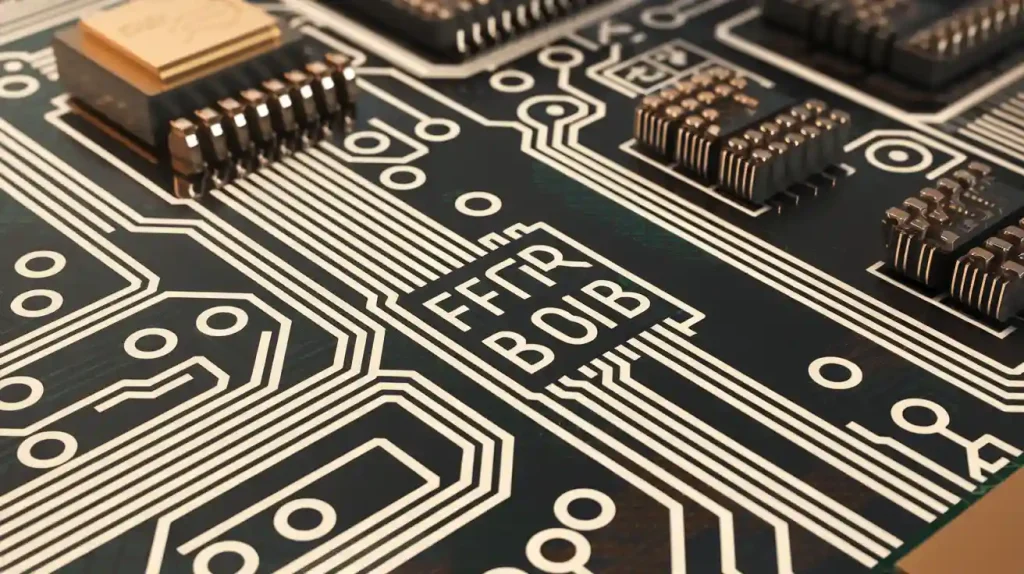
Schematic capture forms the backbone of any successful PCB project. It allows you to translate your circuit design ideas into a clear and structured visual representation. A well-crafted schematic ensures your design is accurate and functional, reducing the risk of errors during manufacturing. By arranging components logically, such as placing power supplies at the top and signal flow from left to right, you can enhance clarity and simplify troubleshooting. Using consistent naming conventions and minimizing wire crossings further improves the schematic’s readability. These practices not only streamline the design process but also help you avoid costly manufacturing defects.

Key Takeaways
Schematic capture helps turn circuit ideas into clear drawings. This reduces mistakes during manufacturing.
Arrange parts in your schematic in a logical way. This makes it easier to understand and fix problems. Use the same naming style for all parts.
Check your design rules (DRC) to find mistakes early. This ensures your schematic follows rules and is ready for PCB layout.
Add clear labels and notes to your schematic. This helps with fixing issues and making changes later.
Work with your team while designing to find mistakes faster. This makes the schematic capture process smoother.
Understanding the Importance of Schematic Capture
What is Schematic Capture?
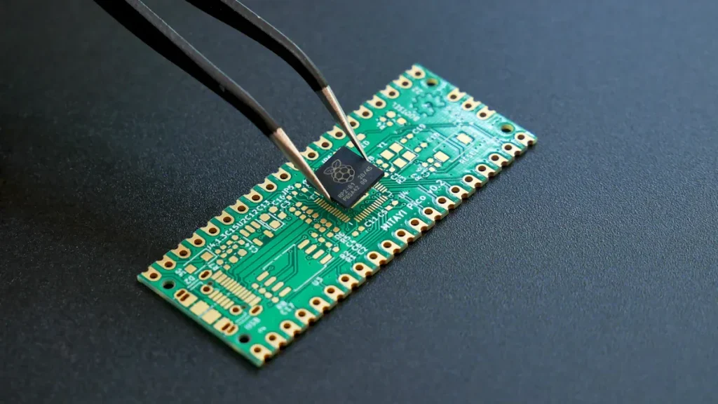
Schematic capture is the process of creating a visual representation of your circuit design. It involves placing electronic components and defining their connections within a schematic. This step forms the foundation of your PCB project, ensuring that your design is both logical and functional. By using schematic capture, you can organize components, establish electrical connections, and prepare your design for the next stages of PCB development.
A schematic acts as a blueprint for your circuit design. It visually depicts how components interact and ensures that every connection is clear and precise. This clarity helps you identify potential issues early, saving time and resources during the design process. Whether you’re designing a simple circuit or a complex PCB, schematic capture is an essential step that sets the stage for success.
The Role of a PCB Schematic in Design and Manufacturing
A PCB schematic plays a critical role in both the design and manufacturing phases of your project. It serves as a universal language, bridging the gap between your design intent and the final product. By visualizing connections beforehand, the schematic helps you identify errors and refine your design before moving to the layout stage.
During manufacturing, the schematic provides a clear roadmap for assembling the PCB. It ensures that the manufacturer understands your circuit’s design intent, reducing the likelihood of errors. A well-documented schematic also becomes a valuable reference throughout the PCB’s lifecycle, aiding in troubleshooting and future modifications.
Benefits of Accurate Schematic Capture
Accurate schematic capture offers measurable benefits in terms of time and cost savings. By reusing schematic designs, you can eliminate the need to recreate complex circuitry, saving valuable time. Additionally, accurate schematics reduce design iteration cycles, minimizing redundant work and optimizing resources.
Benefit Type | Description |
|---|---|
Time Efficiency | Reusing schematic designs saves time by eliminating the need to recreate complex circuitry. |
Cost Savings | Reduces design iteration cycles and minimizes redundant work, optimizing resources and lowering costs. |
Clarity and precision in schematic capture also enhance the overall quality of your PCB. By visualizing connections early, you can identify potential errors and ensure that your design aligns with your project goals. This attention to detail not only streamlines the design process but also helps you deliver a reliable and functional PCB.
Step-by-Step Guide to Creating a PCB Schematic

Setting Up the Schematic Design Environment
Selecting the Right Schematic Capture Software
Choosing the right software is the first step in creating a successful PCB schematic. Look for tools that offer user-friendly interfaces, robust libraries, and advanced features like design rule checks (DRC). Popular options include Altium Designer, KiCad, and Eagle. Each software has unique strengths, so consider your project requirements and budget before making a decision. Early collaboration with engineers and consultants ensures that your chosen software aligns with industry standards and project goals. This step helps you avoid potential challenges later in the design process.
Configuring Libraries and Project Settings
Once you select your software, configure the libraries and project settings. Libraries store the symbols and footprints for your components, so ensure they are accurate and up-to-date. Establishing basic layout and structural elements is crucial at this stage. Programming your project settings, such as grid size and default units, determines the spatial needs and functional requirements of your schematic. These configurations streamline your workflow and ensure consistency throughout the design process.
Adding and Organizing Components
Choosing Components from Libraries
Select components from your software’s libraries based on your schematic’s requirements. Use standardized symbols to ensure clarity and avoid confusion. Group related components together to simplify tracing and understanding. For example, place resistors and capacitors near the ICs they support. Logical signal flow, typically from left to right or top to bottom, enhances readability. Minimize wire crossings by arranging components strategically and using junction dots where necessary.
Placing and Arranging Components
Arrange components on the schematic grid to maintain symmetry and clarity. Start with a block diagram to map out the overall design flow. Place components with higher voltages at the top and lower voltages at the bottom. This logical organization improves signal flow and reduces trace length. Utilize busses to streamline the design and improve readability. Pay attention to alignment and spacing to create a clean and professional schematic.
Defining Electrical Connections
Using Nets to Connect Components
Nets represent the electrical connections between components in your schematic. Clearly illustrate junctions where wires intersect to avoid confusion. Use designated net names instead of numerous connections to enhance readability. For example, label power and ground nets consistently across the schematic. This practice simplifies the design and ensures accurate electrical connections.
Labeling and Organizing Connections
Labeling connections is essential for maintaining a clean and organized schematic. Use consistent notations for component identification and pin labeling. Standardize net and pin names to ensure clarity and ease of understanding. Generate and manually verify netlist files to confirm the accuracy of your electrical connections. These steps help you create a schematic that is both functional and easy to interpret.
Validating the Schematic
Performing Design Rule Checks
Design rule checks (DRC) ensure your schematic adheres to predefined rules and standards. These checks identify issues like overlapping connections, missing nets, or incorrect pin assignments. Most schematic capture software includes built-in DRC tools that automate this process. You can run these checks to catch errors early, saving time during the PCB layout phase.
To validate your schematic effectively, follow these steps:
Review the schematic for duplicate components and misplaced symbols.
Verify that all nets connect properly and follow logical paths.
Check for consistent use of circuit objects, such as power and ground symbols.
Run the DRC tool to highlight any violations or inconsistencies.
By addressing these issues, you ensure your schematic is error-free and ready for the next stage of design.
Identifying and Fixing Errors
Errors in a schematic can lead to costly delays during PCB manufacturing. To fix them, start by reviewing the DRC report. Focus on high-priority issues like missing connections or incorrect component placements. Use the software’s highlighting tools to locate errors quickly.
Collaborate with your team to cross-check the schematic against the design requirements. This step ensures all components and connections align with the project goals. Once you resolve the errors, rerun the DRC to confirm the fixes. Repeating this process guarantees a robust and reliable schematic.
Preparing for PCB Layout
Generating a Bill of Materials (BOM)
A Bill of Materials (BOM) lists all the components required for your PCB. It includes details like part numbers, quantities, and descriptions. To create a BOM, export the data from your schematic capture software. Ensure the BOM includes:
Reference designators for each component.
Component values and specifications.
Manufacturer names and part numbers.
Mounting types (e.g., surface-mount or through-hole).
A well-organized BOM simplifies procurement and assembly, reducing the risk of errors during manufacturing.
Exporting the Netlist for PCB Design
The netlist defines the electrical connections in your schematic and serves as the foundation for PCB layout. Export the netlist in a format compatible with your PCB design software. Common formats include IPC-D-356 and ODB++. These formats ensure accurate data transfer between the schematic and layout stages.
Before exporting, double-check the netlist for completeness and accuracy. This step ensures the PCB layout reflects your schematic’s design intent. A clean and accurate netlist streamlines the transition to the layout phase, saving time and effort.
Best Practices for Schematic Capture
Use Standardized Symbols and Naming Conventions
Using standardized symbols and consistent naming conventions is essential for creating a clear and professional schematic. When you apply uniform labels to components and connections, you make your schematic easier to read and understand. This approach allows you and others to quickly identify potential issues, which is crucial for debugging your PCB design. For example, naming power nets as “VCC” or “GND” across the schematic ensures clarity and avoids confusion during the design and manufacturing stages.
Standardized symbols also help maintain consistency across different projects. They allow team members to collaborate effectively and ensure that your schematic adheres to industry standards. By following these practices, you can create a schematic that is not only functional but also easy to interpret.
Maintain a Clean and Organized Schematic
A clean and organized schematic improves readability and reduces the chances of errors. To achieve this, follow these strategies:
Arrange components logically, with higher voltages at the top and lower voltages at the bottom.
Place components from left to right to maintain a natural flow.
Use busses to simplify connections and enhance clarity.
Standardize net and pin names to ensure consistency.
Begin with a block diagram to outline the overall design before diving into details.
Avoid cluttering your schematic with unnecessary details. Keep power and ground pins visible to prevent unexpected connections. Simplify complex connectors and avoid overly restrictive rules that might hinder creativity. These practices ensure your schematic remains both functional and visually appealing.
Verify Component Specifications
Verifying component specifications is a critical step in schematic capture. Before finalizing your design, double-check that each component meets the requirements of your PCB. Ensure that the voltage, current, and power ratings align with your design’s needs. Cross-reference the specifications with the manufacturer’s datasheets to confirm accuracy.
Incorrect specifications can lead to design failures or damage to your PCB during operation. For example, using a resistor with an insufficient power rating might cause overheating. By verifying specifications early, you can avoid costly mistakes and ensure your schematic translates into a reliable PCB.
Document the Design Thoroughly
Thorough documentation is essential for creating a reliable schematic and ensuring a smooth transition to the PCB layout phase. When you document your design, you provide a clear roadmap for both yourself and others involved in the project. This step minimizes confusion and reduces the likelihood of errors during manufacturing or future modifications.
To document your schematic effectively, include the following elements:
Symbols and Labels: Use standardized symbols for all components and label each one with clear reference designators.
Signal Flow: Arrange the schematic logically, typically from left to right or top to bottom.
Grid Alignment: Align components to a grid to maintain clarity and consistency.
Functional Grouping: Place related components close to each other to simplify tracing.
Minimize Crossings: Avoid crossed wires by arranging components strategically and using junction dots where necessary.
Standardized Notations: Follow industry standards for symbols and reference designators.
Annotation and Documentation: Add notes, a Bill of Materials (BOM), and any other relevant details for clarity.
Review and Verification: Perform a Design Rule Check (DRC) to catch errors before moving to the next stage.
By following these steps, you ensure your schematic is not only functional but also easy to interpret. A well-documented design saves time during the PCB layout process and simplifies troubleshooting later.
Tip: Always include annotations for complex sections of your schematic. These notes help others understand your design intent and make collaboration more effective.
Collaborate and Review with Team Members
Collaboration plays a vital role in creating a robust schematic. When you involve your team in the review process, you gain valuable insights that improve the overall design. Team members can spot errors you might have missed and suggest optimizations for better performance.
Here are some benefits of collaboration during schematic capture:
Increased efficiency and productivity
Improved error detection
Enhanced communication among team members
Streamlined design process
Schematic reviews often involve multiple stakeholders, such as engineers, designers, and project managers. This collaborative effort ensures your schematic is optimized for all aspects of the project. For example, a hardware engineer might identify a potential issue with component placement, while a manufacturing expert could suggest changes to simplify assembly. These inputs lead to a more efficient PCB layout process and reduce the risk of costly errors.
To make the most of team collaboration, schedule regular review sessions and encourage open communication. Use version control tools to track changes and maintain a clear record of revisions. By fostering a collaborative environment, you ensure your schematic meets the highest standards of quality and functionality.
Note: Collaboration is not just about finding errors. It’s also an opportunity to share knowledge and improve the overall design process.
Ensuring an Error-Free PCB Schematic

Avoiding Common Mistakes
Incorrect Pin Assignments
Incorrect pin assignments can disrupt your circuit’s functionality. Always double-check pin configurations against the manufacturer’s datasheet. Misaligned pins, such as swapping power and ground, can cause irreversible damage to components. Use schematic capture software with built-in pin validation tools to catch these errors early. Label each pin clearly to avoid confusion during the design process.
Overlapping or Missing Connections
Overlapping wires or missing connections often lead to circuit failures. Ensure that all nets are properly defined and avoid crossing wires unnecessarily. Use junction dots to indicate intentional intersections. Missing connections, such as a forgotten ground reference, can cause 21% of critical design errors. Always define a single ground reference and verify that all components connect to it. Logical organization and clear labeling reduce the risk of these mistakes.
Tip: Avoid overcrowding your schematic. Adequate spacing between components improves readability and minimizes errors.
Tips for Effective Design Rule Checks
Design rule checks (DRC) act as virtual quality control for your schematic. They ensure compliance with specified requirements and regulatory standards. Follow these steps for effective DRC:
Set minimum trace widths to handle the required current without overheating.
Maintain minimum clearances to prevent shorts and ensure proper solderability.
Verify via sizes to support reliable electrical connections.
Check solder mask clearances to keep pads free of solder mask.
Ensure annular ring sizes meet reliability standards.
Optimize component placement to reduce manufacturing defects.
Route traces to minimize crosstalk and electromagnetic interference.
Running DRC before finalizing your schematic ensures a seamless transition from prototype to manufacturing.
Using Simulation Tools for Validation
Simulation tools help you validate your schematic by analyzing circuit behavior under various conditions. Use DC sweep to study how a DC signal affects circuit response. Small-signal analysis approximates linear responses around an operating point, making it ideal for nonlinear circuits. Sensitivity analysis examines how component tolerances impact performance. Monte Carlo simulations test your design under random variations, ensuring reliability.
These tools identify issues like differential crosstalk, return loss, and insertion loss. By simulating your schematic, you can detect and resolve potential problems before moving to the PCB layout phase.
Note: Incorporating simulation into your workflow reduces unforeseen issues and enhances the reliability of your PCB.
Schematic capture is the cornerstone of successful PCB projects. It ensures your design is accurate, functional, and ready for manufacturing. By following best practices like maintaining logical flow, using busses, and standardizing net names, you can create a clear and reliable pcb schematic. Start with block diagrams to map out your design and simulate circuits to validate performance. Always document your schematic thoroughly to simplify troubleshooting. Applying these techniques will help you streamline your pcb design process and deliver high-quality results.
Tip: Keep power and ground pins visible to avoid unexpected connections and ensure a robust schematic.
FAQ
What is the difference between a schematic and a PCB layout?
A schematic shows the logical connections between components, while a PCB layout represents the physical arrangement of those components on the board. The schematic focuses on functionality, and the layout ensures manufacturability.
Tip: Always validate your schematic before starting the PCB layout to avoid errors.
Can I reuse a schematic for multiple projects?
Yes, you can reuse schematics for similar projects. This saves time and ensures consistency. However, always verify that the reused schematic meets the new project’s requirements and specifications.
Note: Update component values or connections as needed to match the new design.
How do I choose the right schematic capture software?
Choose software based on your project’s complexity, budget, and required features. Popular options include Altium Designer, KiCad, and Eagle. Look for tools with robust libraries, user-friendly interfaces, and design rule check (DRC) capabilities.
Tip: Test free versions or trials before committing to a paid tool.
Why are design rule checks (DRC) important?
DRC ensures your schematic follows predefined rules and standards. It helps you catch errors like missing connections, incorrect pin assignments, or overlapping wires. Running DRC early prevents costly mistakes during PCB manufacturing.
What should I include in my schematic documentation?
Include component symbols, reference designators, net labels, and annotations. Add a Bill of Materials (BOM) and notes for complex sections. Proper documentation ensures clarity and simplifies troubleshooting.
Tip: Use standardized symbols and consistent naming conventions for better readability.