In the developing landscape of modern electronics, 6 layers printed circuit boards (PCBs) represent a critical advancement in multilayer PCB technology. A 6-layer PCB consists of six conductive copper layers separated by insulating dielectric materials, forming a complex sandwich structure that enables superior electrical performance and enhanced functionality. These boards occupy a strategic position in the PCB manufacturing hierarchy offering significantly better performance than 2-layer and 4-layer alternatives while remaining more cost-effective than 8-layer or higher-count designs.
The transition to 6-layer PCBs is driven by the increasing demands of high-speed digital circuits, RF/microwave applications, and complex electronic systems that require exceptional signal integrity, robust power distribution networks, and superior electromagnetic interference (EMI) shielding. Whether you’re an experienced PCB designer evaluating stack-up options, an electrical engineer optimizing signal integrity, or a procurement manager assessing manufacturing capabilities. This article provides the detailed information needed to make informed decisions about 6-layer PCB
What is the Standard 6 Layers PCB Stack-up?
The stack-up configuration of a 6-layer PCB describes how the six copper layers and insulating dielectric materials are organized within the board assembly. This arrangement is essential to achieve optimal electrical performance, signal integrity, and electromagnetic compatibility. Understanding the stack-up is important for PCB designers, as it directly effects impedance control, EMI shielding effectiveness, crosstalk reduction, and overall printed circuit board reliability.
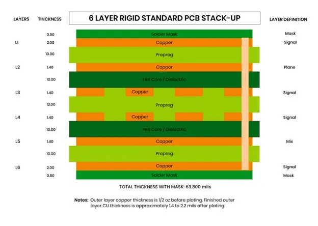
Type 1: Standard Signal-Ground-Signal-Signal-Power-Signal Stack-up (Most Common)
This is the most widely used 6 Layers PCB configuration for general-purpose applications, offering an excellent balance between signal routing flexibility and power integrity.
- Layer 1 (Top Signal – Component Side): Primary signal routing layer where most components are placed. Typically used for high-speed signal traces, critical routing, and surface-mount components.
- Layer 2 (Ground Plane – GND): Continuous ground plane providing return paths for signals on Layer 1, excellent EMI shielding, and reference for controlled impedance traces. Minimizes Layer 1 signal crosstalk and radiation.
- Layer 3 (Inner Signal Layer 1): Internal routing layer for high-speed signals, differential pairs, or sensitive analog signals. Sandwiched between ground and power planes for excellent noise immunity.
- Layer 4 (Inner Signal Layer 2): Additional internal routing layer for complex designs. Can be used for digital signals, mixed-signal separation, or orthogonal routing to Layer 3 to minimize crosstalk.
- Layer 5 (Power Plane – VCC/VDD): Dedicated power distribution plane providing low-impedance power delivery to all components. Can be split into multiple voltage domains (3.3V, 5V, 12V) as needed. Provides return path reference for Layer 6 signals.
- Layer 6 (Bottom Signal – Solder Side): Secondary signal routing layer on the bottom surface. Used for component placement on the reverse side and additional routing capacity.
This configuration excels in applications involving balanced signal routing, strong power distribution, and effective EMI control. The adjacent ground and power planes (Layers 2 and 5) create excellent decoupling capacitance, reducing power supply noise.
Type 2: Dual Ground Plane Stack-up for High-Speed Digital Applications
For designs with crucial high-frequency needs, differential signaling (USB 3.0, HDMI, PCIe), or stringent EMI specifications, a dual-ground-plane configuration offers superior performance:
- Layer 1: Top Signal
- Layer 2: Ground Plane (GND)
- Layer 3: High-Speed Signal Layer
- Layer 4: High-Speed Signal Layer
- Layer 5: Ground Plane (GND)
- Layer 6: Bottom Signal
This layout provides two solid ground planes (Layers 2 and 5), creating optimal conditions for high-speed differential pairs and controlled impedance traces. The dual ground planes offer maximum EMI shielding and reduce ground bounce in high frequency switching applications.
Type 3: Mixed-Signal Stack-up with Analog/Digital Separation
For mixed signal designs containing both sensitive analog circuits and noisy digital logic, physical separation of analog and digital sections is important.
- Layer 1: Top Signal (Mixed)
- Layer 2: Ground Plane (Analog GND / Digital GND split)
- Layer 3: Digital Signal Layer
- Layer 4: Analog Signal Layer
- Layer 5: Power Plane (Analog PWR / Digital PWR split)
- Layer 6: Bottom Signal (Mixed)
This arrangement assigns Layer 3 to digital signals and Layer 4 to analog signals, with separate ground and power plane sections for each domain.
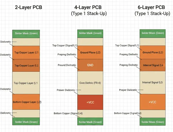
6-Layer PCB vs. 4-Layer PCB vs. 2-Layer PCB: Performance Comparison
Choosing the proper PCB layer count is a significant design decision that effects performance, manufacturability, cost, and time-to-market. This comprehensive comparison examines the key differences between 2-layer, 4-layer, and 6-layer printed circuit boards across multiple performance parameters:
| Performance Factor | 2-Layer PCB | 4-Layer PCB | 6-Layer PCB |
| Signal Integrity | Limited; suitable for <50 MHz | Good; adequate for 50-100 MHz | Excellent; supports >100 MHz, GHz-range signals |
| Impedance Control | Difficult; microstrip only | Moderate; limited stripline | Superior; multiple stripline and microstrip options |
| Power Distribution | Trace-based; high impedance, voltage drop | Dedicated planes; improved stability | Optimal; multiple power/ground planes, minimal noise |
| Thermal Management | Limited copper for heat dissipation | Improved with internal planes | Superior; extensive copper mass aids heat spreading |
| Relative Cost | Lowest (baseline) | 1.5-2x higher | 2-3x higher than 2-layer |
When to Choose 6-Layer PCBs: 6-layer PCBs are the best choice for high-speed digital designs operating above 100 MHz, mixed-signal applications requiring analog/digital isolation, impedance-critical interfaces (USB 3.0, HDMI, PCIe, Gigabit Ethernet), high-density BGA packages, RF/microwave circuits, automotive and industrial applications.
Design Specifications, Materials & Manufacturing Capabilities
Proper material selection and specification definition are critical to achieving optimal performance in 6-layer PCB designs. The following parameters must be carefully considered during the design phase:
Laminate Materials
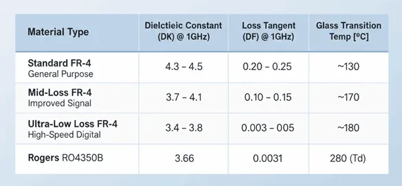
- FR-4 Standard Grades: The most common PCB substrate material, FR-4 (Flame Retardant 4) is a glass-reinforced epoxy laminate. Standard grades include TG130 (glass transition temperature 130°C), TG150 (150°C), and TG170 (170°C).
- High-TG FR-4: TG180 materials offer superior thermal performance for applications experiencing elevated operating temperatures, lead-free soldering processes, or thermal cycling requirements.
- High-Frequency Materials: For RF, microwave, and high-speed digital applications requiring exceptional signal integrity, specialized materials are essential. Rogers RO4003C (Dk=3.38, low loss) and RO4350B (Dk=3.48, very low loss tangent) low dispersion, and minimal signal attenuation at GHz frequencies.
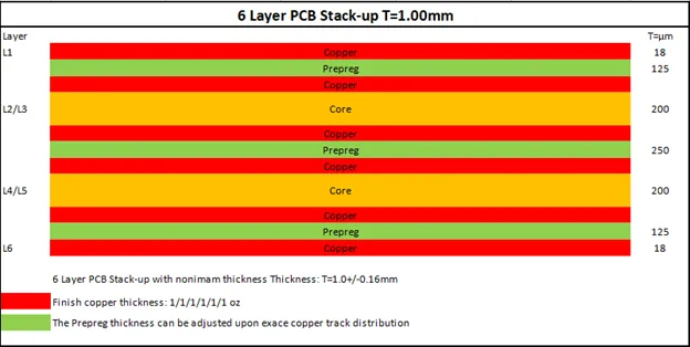
Board Thickness
Standard thickness: 1.6mm (0.063 inches) – the industry standard for most applications, providing good mechanical strength and compatibility with standard assembly equipment.
- Alternative thicknesses: 1.0mm (thinner, for compact devices), 2.0mm (enhanced rigidity), 2.4mm (high-power applications requiring additional copper mass or specific connector requirements).
Copper Weight
- Outer layers: Typically 1oz (35µm or 1.4 mils) for standard designs. 2oz (70µm) copper is used for high-current applications, improved thermal management, or enhanced mechanical strength.
- Inner layers: Commonly 0.5oz (17.5µm) or 1oz. Thinner copper (0.5oz) on signal layers reduces costs and allows finer trace geometries. Power and ground planes typically use 1oz for better current distribution.
Dielectric Constant (Dk) and Loss Tangent
- Dielectric Constant (Dk): Determines signal propagation velocity and impedance. FR-4 typically ranges from Dk=4.2 to 4.5 at 1 MHz, with frequency-dependent variation. High-frequency materials like Rogers provide more stable Dk across frequency ranges.
- Loss Tangent (Df): Measures signal attenuation in the dielectric material. Standard FR-4 has Df ≈ 0.02, while high-frequency materials achieve Df < 0.005. Lower loss tangent is critical for maintaining signal integrity in GHz-range applications.
Via Technology Explained
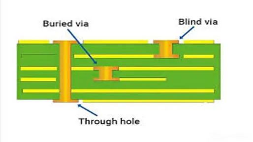
- Through-Hole Vias: The most common and cost-effective via type, extending through all six layers. Ideal for most interconnections and provides excellent reliability. Used when connections are needed across multiple or all layers.
- Blind Vias: Connect an outer layer to one or more inner layers without extending through the entire board. Examples: Layer 1 to Layer 3, or Layer 4 to Layer 6. Used to increase routing density without consuming all layers. Adds moderate cost.
- Buried Vias: Connect only internal layers without reaching either outer surface. Example: Layer 2 to Layer 5. Provides maximum routing flexibility and density for complex designs. Most expensive via option due to additional manufacturing steps.
Solder Mask and Silkscreen
Solder Mask Colors: Green (industry standard, most economical, best for AOI inspection), Blue, Black (aesthetically appealing, good contrast), White, Red, Yellow, Matte Black (premium appearance for consumer electronics)
Silkscreen Colors: White (standard on green, blue, black masks), Black (on white or yellow masks), Yellow (on blue or black masks for high contrast). Silkscreen provides component designators, polarity marks, logos, and assembly instructions.
Primary Applications for 6-Layer PCBs
6-layer PCB technology serves as the backbone for numerous high-performance electronic systems across diverse industries. The major applications of 6-layer PCBs are as follows:
- High-Speed Computing: Computer motherboards, server platforms, workstation boards, GPU cards, and FPGA development boards.
- Telecommunications Equipment: Network switches, routers, fiber optic transceivers, 5G base stations, and cellular infrastructure.
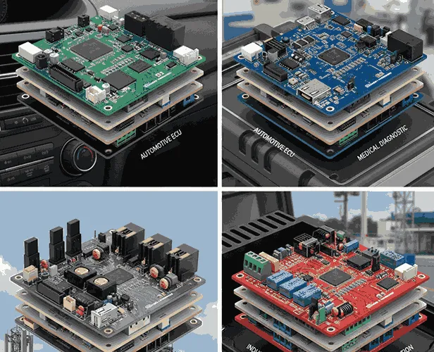
- Automotive Electronics: Advanced Driver Assistance Systems (ADAS), electronic control units (ECUs), infotainment systems, battery management systems for electric vehicles, autonomous driving controllers, and radar modules.
- Industrial Control Systems: Programmable Logic Controllers (PLCs), motor drive controllers, SCADA systems, industrial IoT gateways, robotics controllers, and power electronics
- Consumer Electronics: High-end smartphones, tablets, gaming consoles, virtual reality headsets, smart home hubs, and professional audio/video equipment.
- RF/Microwave Applications: Radar systems, wireless communication transceivers, satellite communication equipment, spectrum analyzers, and test equipment.
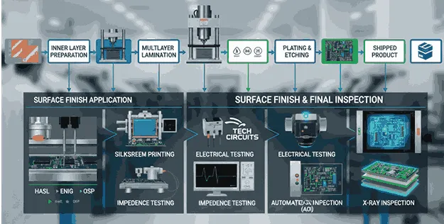
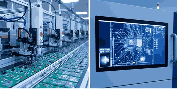
Manufacturing Process of 6-Layer PCB
Understanding the 6-layer PCB manufacturing process helps designers appreciate the complexity involved and optimize designs for manufacturability. The process involves multiple precision steps:
1. Inner Layer Fabrication
Manufacturing begins with inner layers (L2, L3, L4, L5). Copper-clad core material is coated with photosensitive resist (dry film), exposed to UV light through photomasks containing the circuit pattern, and developed to reveal the copper pattern.
2. Oxide Treatment
Inner layer copper surfaces undergo brown oxide or black oxide chemical treatment to improve adhesion during lamination. This micro-rough surface texture ensures strong bonding between copper layers and prepreg materials, critical for reliability and prevention of delamination.
3. Lamination Process
The stack-up is assembled in a clean room environment: inner core layers (with copper circuits), prepreg sheets, and outer copper foils are carefully stacked according to the designed stack-up. This assembly is placed in a lamination press where heat (typically 170-180°C) and pressure (300-400 PSI) are applied for 60-90 minutes.
4. Drilling and Via Formation
After lamination, holes are drilled for component leads and vias. CNC drilling machines with carbide or diamond-coated drill bits create throat holes with tolerances of ±0.05mm. For blind and buried vias, controlled-depth drilling or laser drilling is employed. Laser drilling (CO₂ or UV laser) creates microvias as small as 0.1mm diameter.
5. Copper Plating
Drilled holes are metallized through electroless copper plating, which deposits a thin conductive copper layer on non-conductive hole walls. This is followed by electrolytic copper plating to build up copper thickness to the specified level (typically 20-25µm in holes).
6. Outer Layer Imaging and Etching
Similar to inner layer processing, outer layers (L1 and L6) are coated with photoresist, exposed through photomasks, and developed. The exposed copper is then etched away, leaving the final circuit pattern, pads, and traces.
7. Solder Mask Application
Liquid photo imageable solder mask (LPI) is applied to both sides of the board, covering all areas except pads and test points. The solder mask is exposed through photomasks to cure in desired areas, then developed to remove uncured mask from pad areas.
8. Surface Finish and Final Inspection
The selected surface finish (HASL, ENIG, OSP, etc.) is applied to exposed copper pads. Silkscreen legend is printed for component designators, polarity markings, and company logos. The board undergoes electrical testing (flying probe or fixture testing) to verify continuity and isolation. For impedance-controlled designs, TDR testing verifies impedance values. Automated Optical Inspection (AOI) checks for defects. X-ray inspection may be performed to verify internal via quality and layer alignment.
Cost Factors: Understanding 6-Layer PCB Pricing
6-layer PCB pricing is influenced by numerous factors related to design complexity, materials, manufacturing processes, and order volume. Understanding these cost drivers enables informed decision-making and design optimization:
Quantity Impact
Order quantity dramatically affects unit pricing due to setup costs, tooling, and manufacturing efficiency:
- Prototype (1-10 pieces)
- Small Batch (50-100 pieces
- Mass Production (500+ pieces
Material Selection
- Standard FR-4 (TG130-150): Baseline pricing, most economical
- High-TG FR-4 (TG170-180): Adds 10-20% to material cost
- Rogers high-frequency materials: Premium pricing, 2-5x cost of standard FR-4. RO4003C and RO4350B are among the most economical high-frequency options.
- Hybrid constructions: Combining FR-4 core layers with Rogers prepreg for specific layers balances cost and performance.
Board Size and Panel Utilization
Manufacturers process PCBs on standard panel sizes (typically 18″ × 24″ or 21″ × 24″). Efficient panel utilization significantly reduces cost. Boards that fit evenly into panels (e.g., 100mm × 100mm boards can fit multiple per panel) are more economical than odd-sized boards with poor panel utilization.
Copper Weight
- Standard 1oz copper: Baseline pricing
- 2oz copper: Adds 20-40% to cost due to additional plating time and material
- Heavy copper (3oz+): Significant cost increase, specialized processing, longer lead times
Cost Reduction Strategies
- Use standard specifications (1.6mm thickness, 1oz copper, standard FR-4, green solder mask, HASL finish) whenever possible
- Optimize board dimensions for efficient panel utilization
- Avoid blind/buried vias unless absolutely necessary for routing or density requirements
- Consolidate orders—larger quantity orders significantly reduce per-unit cost
- Use standard lead times—avoid rush charges unless critical to the project timeline
- Work with the manufacturer’s design review to identify cost-saving opportunities early
Quality Control and Testing for 6-Layer PCBs
Rigorous quality control and testing procedures ensure 6-layer PCBs meet design specifications and reliability requirements. Comprehensive testing at multiple manufacturing stages identifies defects before boards reach assembly:
Electrical Testing
- Flying Probe Test
- Fixture-based Test (Bed of Nails)
Automated Optical Inspection (AOI)
High-resolution cameras scan outer layers to detect defects such as: missing copper (open circuits), copper shorts (bridging), incorrect trace width or spacing, solder mask defects, silkscreen errors, surface contamination. AOI systems compare actual board images against design data (Gerber files) to identify deviations.
X-Ray Inspection
X-ray systems provide non-destructive inspection of internal structures not visible from the surface. X-ray inspection verifies via formation and copper plating quality inside holes, layer-to-layer registration accuracy (alignment between internal layers), absence of voids in vias and barrel plating, buried via quality in designs using complex via structures.
Why Choose Wonderful PCB for 6-Layer PCB Manufacturing
Wonderful PCB stands as your trusted partner for high-quality 6-layer PCB manufacturing, combining advanced capabilities, technical expertise, and customer-focused service:
Advanced Manufacturing Capabilities
Our state-of-the-art production facilities feature cutting-edge equipment for multilayer PCB fabrication. We maintain precision tolerances for fine-pitch designs, support complex via structures including blind and buried vias, and offer controlled impedance manufacturing with TDR testing verification.
Experienced Engineering Support
Our engineering team provides a comprehensive Design for Manufacturing (DFM) review to identify potential issues before production, optimizing your design for manufacturability and cost-effectiveness. We offer stack-up design assistance, helping you select the optimal layer arrangement and materials for your specific application.
Quality Assurance
Wonderful PCB maintains ISO 9001 certification and UL recognition, demonstrating our commitment to quality management systems and safety standards. Every board undergoes rigorous electrical testing, AOI inspection, and adherence to IPC-A-600 workmanship standards.
Competitive Pricing
We offer transparent, competitive pricing with volume discounts that scale with your production needs. Our online quotation system provides instant pricing for standard specifications, while our sales team works with you on custom quotations for specialized requirements. We believe in value-based pricing—delivering premium quality at fair market rates without hidden fees or surprise charges.
Complete PCB and PCBA Services
As a true one-stop solution, Wonderful PCB offers comprehensive services from bare board fabrication through complete assembly. Our integrated approach includes: PCB design support and layout services, bare board manufacturing with full quality testing, component sourcing and procurement, SMT and through-hole assembly, functional testing and quality inspection, conformal coating and potting services, box build and system integration.
Conclusion
6-layer Printed Circuit Boards (PCBs) shows the optimal solution for modern electronic designs lacking superior performance, signal integrity, and electromagnetic compatibility. As we have explored throughout this comprehensive guide, the strategic advantages of 6-layer construction including multiple signal routing layers, dedicated power and ground planes, exceptional EMI shielding, and superior thermal management make these boards the preferred choice for high-speed digital systems, RF/microwave applications, automotive electronics, industrial controls, and countless other demanding applications.
While 6-layer PCBs command a cost premium over simpler 2-layer and 4-layer alternatives, this investment delivers tangible returns through enhanced reliability, improved signal quality, reduced system complexity, and often smaller board sizes due to increased routing density.
Ready to get started?
Contact Wonderful PCB today for a quote, DFM analysis, or technical consultation. Upload your design files to our online system for instant pricing or speak with our engineering team to discuss your specific requirements.