You might ask what the vlsi design cycle is. This process helps you make a working chip step by step. In very large scale integration, you use semiconductor technology. This lets you put millions of transistors on one chip. Each stage in the cycle is important. If you skip a step, you might get errors or a chip that does not work. The vlsi field has grown very fast. The global market was worth about USD 634.85 billion in 2025. It may reach USD 1,055.39 billion by 2034. You usually follow these main stages in the cycle:
Requirement gathering
System-level design
RTL design
Functional verification
Synthesis
Place and route
Physical verification
Semiconductor technology affects the electronics you use every day.
Specification
The specification phase is the first step in the vlsi design cycle. Here, you decide what the chip should do. You also decide how well it should work. This step helps you make good choices later. If you do this step well, your chip will likely work. You can also avoid big mistakes and save time.
Requirements
You must have clear requirements before you start vlsi chip design. These requirements tell what the chip should do. They also tell how fast, how much power, and how big the chip should be. You list all the features the chip needs. Writing these details helps everyone know the goals. It makes sure the design fits what people want.
Tip: Write requirements in easy words. Use short sentences. Try not to use hard words.
Many teams use different ways to organize their requirements. Here is a table with some common methods:
Methodology | Description |
|---|---|
SystemVerilog | Has many tools for checking if the chip works. It uses object-oriented programming and random testing. |
Universal Verification Methodology (UVM) | Uses SystemVerilog. It helps teams build tests that can be used again. |
VHDL | Used a lot for writing and checking chip designs. It helps model and test hardware. |
e (Specman) | Has strong tools for checking chips. It uses random testing with rules. |
C/C++ and Python | Used to make test systems and test benches. |
System Goals
You set system goals to help guide the design. These goals include how fast the chip should be. They also include how much it should cost and how much power it can use. You decide how the chip will work with other devices. You also plan for changes in the future. Setting goals helps the team stay on track.
The specification phase is very important in vlsi chip design. It sets the base for the whole process. A good specification makes sure the chip does what it should. This is key for the project to succeed.
Architecture
System Design
You start the architecture phase by planning how your chip will work. You decide what each part of the chip will do. You also choose how these parts will talk to each other. This step helps you break a big problem into smaller, easier tasks. You look at what the chip must do and pick the best way to organize its parts.
You can pick from several architectural styles. Each style has its own strengths. Some styles let you make a chip from scratch. Others use ready-made parts to save time. Here is a table that shows some common styles and what makes them special:
Architectural Style | Description |
|---|---|
Full-Custom Design | You build the whole chip from the ground up. This gives you the best speed and power use, but it takes a lot of time and skill. |
Semi-Custom Design | You use some ready-made parts and some custom parts. This saves time and still gives good results. |
Programmable Logic Devices (PLD) | You can change how the chip works after you make it. This is great for testing ideas quickly. |
System-on-Chip (SoC) Design | You put many parts on one chip. This makes the chip small and fast. You see this in phones and smart devices. |
Off-the-shelf Design | You use parts that are already tested and ready to use. This is quick and works well for many products. |
Tip: Pick an architecture that matches your project’s needs. Think about speed, power, and how much time you have.
Your choice of architecture affects how much power your chip uses and how fast it works. You can use special tricks to save power and boost speed. Here are some ways you can do this:
Technique | Description |
|---|---|
Use Low-Power Components | Pick parts that use less energy. This helps if your chip runs on batteries. |
Power Gating | Turn off parts of the chip when you do not need them. |
Dynamic Voltage and Frequency Scaling (DVFS) | Change the chip’s speed and power use based on what it is doing. |
Duty Cycling | Only turn on circuits when you need them. |
Minimize Signal Switching | Reduce how often signals change to save energy. |
Optimize Load Capacitance | Lower the load on outputs to use less power. |
Multi-Threshold CMOS (MTCMOS) | Use different types of switches to save power in key areas. |
Power-Aware Synthesis | Set your tools to focus on saving power when you build the chip. |
Clock Gating at RTL | Stop the clock in unused parts to cut down on wasted energy. |
Body Biasing | Change voltages to lower leaks and save power. |
Hierarchical Power Domains | Split the chip into zones to control power better. |
Use of FinFET Technology | Use special transistors that leak less and work well at low power. |
Block Diagram
You draw a block diagram to show how your chip works. This diagram uses simple shapes to show each part of the chip. You connect these shapes with lines to show how data moves. A good block diagram helps everyone understand the chip’s plan.
When you make a block diagram, you should:
Show all main parts of the chip.
Draw clear lines for data flow.
Label each block with its job.
Keep the diagram simple and easy to read.
A clear block diagram helps you spot problems early. It also helps your team talk about the chip and make changes before you start building.
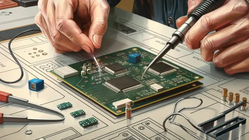
RTL Design
The rtl design stage is where you turn your ideas into code that describes how your chip works. You use a language like Verilog or VHDL to write this code. You focus on how data moves and how each part of the chip behaves. This stage is important because it sets the rules for how your chip will operate.
RTL Coding
You start rtl design by writing code that shows what each block does. You do not worry about the physical layout yet. You describe the logic and how signals flow. You use simple statements to show how the chip should respond to inputs. You make sure each part works together as planned.
Tip: Write clear and simple code. Use comments to explain tricky parts. This helps you and your team understand the design later.
You face several challenges during rtl design. Here is a table that shows the most common ones:
Challenge | Description |
|---|---|
Design Complexity | You must manage large designs. More parts mean more chances for mistakes and longer work times. |
Ensuring Design Correctness | You need to check that your code matches what you want the chip to do. |
Managing Power Consumption | You look for ways to save energy while keeping the chip working well. |
You must pay attention to these challenges. If you do not, you might end up with errors or a chip that uses too much power.
Functional Verification
After you finish rtl coding, you move to design verification. You test your code to make sure it works as expected. You use testbenches and simulation tools. You check every part of the rtl design to find mistakes before you build the chip.
You run many tests to see if the chip responds correctly. You look for bugs and fix them early. Design verification helps you avoid costly errors later. You repeat this process until you feel confident that your rtl design matches your goals.
Note: Good design verification saves time and money. You catch problems before they become bigger issues.
You need to remember that rtl design is a key step in making a reliable chip. Careful coding and strong design verification help you build a chip that works well and meets your needs.
VLSI Design Flow Overview
When you start learning about the vlsi design cycle, you will see that the vlsi design flow gives you a clear path from an idea to a working chip. This flow helps you avoid mistakes and makes sure your chip design works as planned.
Stages in vlsi design flow
You will follow a set of steps in the vlsi design flow. Each step builds on the last one. Here is the usual order you will see in the flow:
Conceptualization and Specification
Architectural Design
Logic Design
RTL Synthesis
Netlist and Floorplanning
Placement and Routing
Physical Verification
Timing Analysis
Extraction and Simulation
Tapeout
Key Activities
You will notice that each stage in the flow has a special job. The vlsi design flow starts with a clear plan and ends with a real chip. You check your work at every step. This helps you find problems early. You can fix them before they grow. The flow includes steps like specification, design entry, synthesis, verification, layout, and fabrication. Each one helps you make sure your chip design is correct. This careful cycle keeps errors low and quality high.
You will see that the flow is your guide for every vlsi project. By following the flow, you make your chip design strong and reliable. The flow is the backbone of every successful vlsi chip.
Logic Synthesis
RTL to Gates
Logic synthesis is a key step in turning your ideas into real hardware. In this stage, you take your RTL code and change it into logic gates. You use special tools to do this job. These tools read your RTL code and create a network of gates that can be built on a chip.
You will see three main steps in logic synthesis:
Translation: The tool changes your RTL code into a form that uses Boolean equations. This step does not depend on the chip technology.
Optimization: The tool makes the Boolean equations simpler. It uses methods like sum of products to do this.
Technology Mapping: The tool matches the optimized equations to real gates from a library. It picks gates that fit your design needs.
Tip: Always check your RTL code for errors before you start synthesis. Clean code helps you get better results.
Optimization
Optimization helps you get the best chip for your needs. You want your chip to be small, fast, and use little power. Logic synthesis tools help you reach these goals by making smart choices during the process.
Here is a table that shows how optimization affects your chip:
Aspect | Impact on VLSI Chips |
|---|---|
Area Optimization | Reduces physical footprint, allowing more chips on a wafer, leading to higher yield and lower costs. |
Speed Optimization | Faster networks often result in larger area consumption, necessitating trade-offs between speed and area. |
Energy Consumption | Larger gates increase capacitance, leading to higher energy consumption during switching. |
You need to balance area, speed, and energy use. If you make your chip faster, it might get bigger and use more power. If you make it smaller, it might run slower. Good logic synthesis helps you find the best balance.
Area optimization lets you fit more chips on a wafer. This lowers costs and lets you add more features.
Speed optimization makes your chip work faster, but it can use more space and energy.
Efficient use of space is important for adding new functions without hurting performance.
You use logic synthesis in every vlsi project. It shapes your design and helps you build chips that work well in the real world.
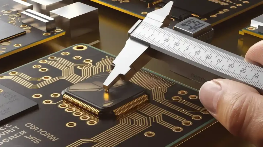
Physical Design

The physical design stage is where you turn your chip’s logic into a real layout. You decide where each part of the chip will go and how wires will connect them. This step is important in vlsi physical design because it shapes how well your chip works and if it can be made without problems.
Floorplanning
You start the physical design stage with floorplanning. Here, you divide the chip into blocks and give each block its own space. You think about how big each block should be and where to put it. Good floorplanning helps you avoid crowded areas and makes sure signals travel quickly. You also plan space for power and clock lines. This step sets the structure for the rest of the vlsi physical design process.
Many tools help you with floorplanning and other tasks in this stage. Some of the most popular tools include:
Synopsys IC Compiler II: Fast place and route, power-aware design.
Mentor Graphics Calibre: Checks rules and matches layout to the schematic.
ANSYS RedHawk: Checks power and reliability.
Tanner Tools: Good for analog and mixed-signal layout.
Avanti Hercules: Checks signal and power integrity.
OpenROAD: Open-source tool for physical design.
KLATencor L-Edit: Used for custom IC layout.
Tip: Choose a tool that fits your project’s needs and your team’s skills.
Placement & Routing
After floorplanning, you move to placement and routing. You place each cell or block in its spot. You want to keep related blocks close together. This helps signals move faster and saves power. You also make sure the chip does not get too hot.
Next, you route the wires. You draw paths for signals to travel between blocks. You balance speed and avoid crowded paths. You also check that your layout follows the rules for making chips. These steps help your chip work well and make it easier to manufacture.
You follow these main steps in the physical design stage:
Partition and floorplan the chip.
Place cells and blocks.
Build the clock tree.
Route the wires.
Check rules and manufacturability.
Optimize power.
When you finish the physical design stage, you have a layout ready for manufacturing. This step is key for every vlsi project.
Design for Testability
When you work on a vlsi chip, you want to make sure you can test it easily. Design for testability helps you find problems early and fix them before the chip reaches customers. You add special features to your chip so you can check if everything works as planned. These features make testing faster and help you save money during production.
Test Features
You use several techniques to improve testability in your chip. These methods help you catch faults and make sure your chip works well.
Scan design lets you control and check the flip-flops inside your chip during tests.
Boundary scan helps you test connections between chips on a board without using probes.
Built-In Self-Test (BIST) adds test hardware inside the chip so it can test itself.
Memory BIST (MBIST) checks the memory blocks inside your chip.
ATPG (Automatic Test Pattern Generation) creates patterns that help you find faults after manufacturing.
These features increase test coverage and reduce the time needed for testing. You can find faults quickly and avoid sending bad chips to customers.
Tip: Add test features early in your design process. This makes testing easier and lowers costs.
You see many benefits when you use these techniques. The table below shows how design for testability helps your chip:
Benefit | Description |
|---|---|
Fault Detection | |
Manufacturing Yield Improvement | You fix problems during production and get more good chips. |
Reliability | You make sure your chip works well for a long time. |
You can test complex chips faster and more accurately. You deliver high-quality chips that work as expected.
Scan Chains
Scan chains play a big role in testing vlsi chips. You connect flip-flops in a chain so you can set and read their values during tests. This setup lets you check the inside of your chip without taking it apart.
You use scan chains to find faults in logic blocks. You control each flip-flop and see how signals move through your chip. This method helps you spot problems that normal tests might miss.
By adding scan chains, you make your chip easier to test and more reliable. You also reduce the risk of costly failures after your chip goes into products.
Note: If you plan your scan chains well, you can save time and improve the quality of your chip.
Integrating design for testability early helps you lower test time and avoid expensive mistakes. You build chips that last longer and perform better.
Timing Analysis
Timing analysis helps you make sure your chip works at the right speed. You use this step to check if signals move through your chip fast enough. If you skip timing analysis, your chip might not work as planned. In vlsi, timing analysis is one of the most important checks before you finish your design.
Static Timing
You use static timing analysis (STA) to check the timing of your chip without running test patterns. STA looks at every path in your circuit and checks if signals arrive on time. This method helps you find problems early. You do not need to use input vectors, so you can check all possible paths quickly.
Here are some common timing analysis methods you might use:
Static Timing Analysis (STA)
Dynamic Timing Analysis (DTA)
Statistical Static Timing Analysis (SSTA)
Sign-off timing analysis
Multi-corner and multi-mode (MCMM) analysis
On-chip variation (OCV) analysis
STA plays a big role in preventing timing violations. You want signals to reach flip-flops and registers at the right moment. If signals arrive too late or too early, your chip could fail. Over 80% of design failures in silicon happen because of timing violations. STA helps you avoid these costly mistakes.
Note: Static timing analysis checks the maximum speed of your chip and makes sure all signals arrive on time. This step is vital for a working chip.
Timing Closure
Timing closure is the process where you fix all timing problems in your chip. You want every signal to meet its timing goal. You might need to change your design, move blocks, or adjust wire lengths. Timing closure can take a lot of effort, but it is key for a working chip.
You follow these steps to reach timing closure:
Analyze timing reports from STA.
Find paths that fail timing.
Change your design to fix these paths.
Run STA again to check if you fixed the problems.
Repeat until you reach timing closure.
You might use special tools to help with timing closure. These tools show you which paths need work. You can change your design and see results quickly. Timing closure makes sure your chip will work at the speed you want.
Tip: Start working on timing closure early. Fixing timing problems at the end can be very hard.
You need timing closure before you can finish your vlsi design. This step gives you confidence that your chip will work in real life.
Physical Verification
Physical verification checks if your chip’s layout is ready to make. You want to be sure your chip will work and follow all the foundry’s rules. This step helps you find mistakes before making the chip. You use different checks to see if your layout is safe and correct.
Here is a table that lists the main steps in physical verification and what they do:
Verification Step | Purpose |
|---|---|
Design Rule Check (DRC) | Checks if the layout follows the foundry’s rules for width and spacing. |
Layout vs Schematic (LVS) | Makes sure the layout matches the circuit plan, or schematic. |
Electrical Rule Check (ERC) | Finds electrical problems like missing wires or too much capacitance. |
DRC
You begin with Design Rule Check, called DRC. This check looks at your chip’s layout and compares it to the foundry’s rules. These rules say how wide wires must be and how far apart they should stay. If you break these rules, your chip might not work or could be hard to make.
DRC is part of physical verification. It helps you find problems like wires that are too close or shapes that are too small. Fixing these problems makes your chip easier to build and more dependable.
Process | Focus | Purpose |
|---|---|---|
DRC | Physical Verification | Makes sure the chip can be made by following design rules. |
Tip: Always run DRC before you finish your layout. This step saves time and money.
LVS
After DRC, you do Layout vs Schematic, or LVS. This check makes sure your layout matches your circuit plan. You want every wire and part in your layout to match your schematic.
LVS is about electrical verification. It checks if your chip will work as you planned. If LVS finds something wrong, you need to fix it before moving on.
Process | Focus | Purpose |
|---|---|---|
LVS | Electrical Verification | Makes sure the layout matches the schematic for correct work. |
Physical verification is an important part of the vlsi process. When you use DRC and LVS, you make sure your design is right and ready for the next step.
Fabrication
After you finish tapeout in the vlsi design cycle, you start fabrication. This step makes your chip design into a real thing. Your ideas turn into silicon chips. These chips go into phones, computers, and other devices.
Wafer Processing
Wafer processing is the first part of making chips. You use a thin piece of silicon called a wafer. You follow many steps to build layers and circuits on it. Each step adds something important to your chip.
Here are the main wafer processing steps:
Surface Cleaning
You clean the wafer to get rid of dust.Initial Oxidation
You grow a thin oxide layer on the wafer.CVD Deposition
You put new materials on the wafer with special gas.Coating Photoresist
You cover the wafer with a material that reacts to light.Metallization and Interconnection
You add metal to connect parts of the chip.Chemical Mechanical Polishing (CMP)
You polish the wafer to make it flat and smooth.Final Testing and Packaging
You test the chip and get it ready for its package.
You might repeat some steps to make complex chips. Each stage helps you build a chip that matches your plan.
Tip: Careful wafer processing stops defects and makes better chips.
Foundry Steps
After wafer processing, you send your chip to a foundry for tapeout. Each foundry uses its own ways to make chips. They have different business styles, technology, and research goals.
Here is a table that shows what top manufacturers do:
Manufacturer | Business Model | Process Node Focus | R&D Focus |
|---|---|---|---|
TSMC | Pure-play foundry | Smaller process nodes | Making process nodes better and improving yields |
Intel | Vertical integration | Getting back tech lead | New packaging, AI chips, quantum computing |
Samsung | Foundry and memory chip | Advanced nodes | New ideas in memory and logic chips |
You pick a foundry that fits your needs. Some foundries make smaller and faster chips. Others work on new packaging or special features. Your tapeout step depends on what the foundry does best.
Fabrication is a very important part of the vlsi design cycle. You must follow every step to get good chips after tapeout.
Testing & Packaging
Electrical Testing
You must check every chip before it leaves the factory. Electrical testing makes sure your chip works as planned. This step helps you find problems from making the chip. You use different ways to test chips. Some common ways are:
Fault modeling
Automatic Test Pattern Generation (ATPG)
Boundary scan testing (JTAG)
Functional testing
Parametric testing
DFT lets you add special features when you design the chip. These features make testing simple. Built-In Self-Test (BIST) lets the chip test itself. You do not need extra tools for this. ATPG makes test patterns to find faults fast. These methods help you save money and time. You can fix problems before customers get the chip. Good testing means only working chips go to users. This keeps people happy.
Tip: Electrical testing helps you find defects early. It makes sure your vlsi chip works well.
Packaging Methods
After testing, you must protect your chip and connect it. Packaging does this job for you. The way you package a chip affects how well it works. It also affects how long it lasts. You need to think about heat, power, and signals.
Interconnect technology is important in packaging. Micro-bumps, through-silicon vias (TSVs), and redistribution layers (RDLs) help connect the chip. Micro-bumps are good for chip-to-substrate links. But they can have problems with heat and shaking. Electromigration and thermal migration can hurt reliability.
TSVs let signals and heat move up and down in the chip. This helps the chip work better. But different materials can crack or break when the chip gets hot or cold.
To make packaging better, you must study heat, electricity, and force. Using new materials like high-density interconnects and advanced thermal materials helps control heat. It also makes the chip last longer. As chips get faster and smaller, good packaging design matters more.
You can see that testing and packaging are both important. They help your chip work well and last a long time.
Silicon Validation
When you finish making a chip, you need to check if it works as planned. This step is called silicon validation. You want to make sure your chip matches the original design and works well in real life.
Post-Fabrication Checks
After fabrication, you test the first chips that come from the factory. These chips are called prototypes. You place them on special boards and run many tests. You look for problems that did not show up during earlier checks. Sometimes, bugs escape the first round of testing. Now, you can find them because the chip runs at real system speed.
You follow a standard process for silicon validation:
Pre-silicon verification uses software to test your chip before it is made. You run test cases in a simulator. This step checks if your RTL code matches the specification.
Post-silicon validation starts after you get the real chip. You test the chip on hardware. You see how it works in real time and in real conditions.
Note: Post-silicon validation helps you find issues that only appear when the chip runs at full speed or in a real environment.
Final Product
Once you finish all checks, you know if your chip is ready for the market. You look at how the chip performs, how much power it uses, and if it meets all your goals. If you find problems, you can fix them before making more chips.
Here is a simple table to show the difference between pre-silicon and post-silicon steps:
Step | When It Happens | What You Test On | Speed of Testing |
|---|---|---|---|
Pre-silicon Verification | Before fabrication | Software simulator | Not real system speed |
Post-silicon Validation | After fabrication | Real hardware | Real system speed |
You need silicon validation to make sure your vlsi chip works as you planned. This step gives you confidence that your design will succeed in the real world.
You make vlsi chip design more reliable by following every stage. This way, you can avoid mistakes and keep your work steady. Knowing the vlsi design flow helps you improve speed, size, and power use. New things like AI-driven automation and 3D integration are changing vlsi’s future. If you want to grow in your job, learn new skills, get certificates, and talk to experts. The cycle helps you build better chips and stay ahead in tech.
Trend | Impact on Semiconductor Technology |
|---|---|
AI-driven design automation | Makes chip designs faster and easier |
Power optimization strategies | Helps small devices work better |
3D integration techniques | Gives better speed and heat control |
Security-first approaches | Keeps chips safe from hackers |
Advanced simulation tools | Checks designs faster and more accurately |
Check what you know and fix weak spots.
Take special classes.
Meet and talk with people in the field.
FAQ
What is the vlsi design cycle?
You follow the vlsi design cycle to create a chip step by step. This cycle helps you plan, build, and test your chip. Each stage makes sure your chip works well and meets your needs.
Why does vlsi matter in electronics?
You use vlsi to fit millions of tiny parts on one chip. This makes devices smaller, faster, and smarter. Phones, computers, and cars all use vlsi chips to work better.
How do you start a design project?
You begin by writing down what you want your chip to do. You set clear goals and list features. This helps you and your team stay focused and avoid mistakes.
What tools help with vlsi design?
You use special software to draw, test, and check your chip. Tools like Synopsys, Mentor Graphics, and Cadence help you design, simulate, and verify your chip before making it.
Can you fix mistakes after making a chip?
You can find and fix some mistakes during testing. If you find big problems, you may need to change your design and make a new chip. Careful planning helps you avoid costly errors.