Ensuring the reliability of electronic product designs is crucial. Manufacturability design encompasses three key aspects: PCB manufacturability design, PCBA assembly design, and cost-effective manufacturing design. Among these, PCB manufacturability design focuses on the manufacturing perspective of PCB boards, considering process parameters to improve production yield and reduce communication costs. Design considerations include line width and spacing, hole-to-line and hole-to-hole distances, all of which must be addressed during the design phase.
The Importance of PCB Design
In electronic product development, the PCB serves as the physical medium for the design content, realizing all design intentions and product functions. Therefore, PCB design is an indispensable link in any project. Manufacturability design of PCBs requires engineers’ attention to ensure that the design aligns with manufacturing capabilities.
Common Design Pitfalls
After completing PCB design, the physical circuit board is produced. Often, the designed PCB cannot be manufactured due to mismatches between the design process and production equipment. Design engineers must understand the production process capabilities during the design phase to avoid such issues.
Role of DFM Analysis
Design for Manufacturability (DFM) analysis software performs manufacturability checks on the designed PCB according to production process parameters. It helps design engineers identify potential manufacturability issues before production, serving as a bridge between design and manufacturing.
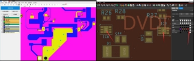
DFM Inspection Item Case Studies
wonderfulpcb DFM Services manufacturability analysis software has developed 19 major items and 52 detailed inspection rules for PCB bare board analysis. These rules cover a wide range of potential manufacturing problems. Below are some classic cases where DFM analysis has assisted users in resolving issues:
1. Allegro Design File Short Circuit
In the DFM electrical network inspection, a short circuit between the power supply and the ground was detected. Upon checking the PCB file in Allegro, it was found that the heat dissipation ground holes of two SMD pads were short-circuited with the power layer, and the ground holes were not isolated in the power layer, resulting in a short circuit.
2. PADS Design File 2D Line Short Circuit
The DFM electrical network check revealed a short circuit between power supply and ground. Verification by the layout engineer showed that a 2D line on the fifth layer was not canceled when converting the Gerber file, leading to a short circuit in the electrical network.

3. Altium Design File Open Circuit
The DFM electrical network check identified an open circuit in the entire ground network on the second layer. Using Altium Designer to open the file revealed that the entire ground holes were isolated from the copper foil, causing an open circuit in the ground network.

4. Solder Mask Window Missing
The DFM solder mask window abnormality inspection found that the solder mask was missing in areas intended for soldering. Without a window in the solder mask, the area cannot be soldered, leading to potential assembly issues.
5. Missing Drilling
The missed drilling analysis inspection identified missing holes for DIP device pins. Without these holes, DIP devices cannot be inserted and soldered. If drilling is performed later, the hole may lack copper plating, resulting in an open circuit that cannot be remedied.
DFM Detection Functions
1. Circuit Analysis
Minimum Line Width: Design engineers must ensure trace widths are adequate to handle the expected current. Insufficient trace width can lead to overheating and potential failure.
Minimum Spacing: Adequate spacing between traces is essential to prevent short circuits and signal interference. Spacing should meet voltage requirements and manufacturing capabilities.
SMD Spacing: Proper spacing between SMD pads is crucial to prevent solder bridges and ensure reliable connections.
Pad Size: Pad dimensions affect soldering quality. Pads that are too small can result in poor solder joints, while excessively large pads may cause component misalignment.
Grid Copper Plating: While grid copper plating can enhance heat dissipation, excessively small grid spacing and line width can complicate manufacturing processes.
Hole Ring Size: Adequate hole ring size is necessary for proper soldering. Small hole rings can lead to soldering difficulties, while small via hole rings may cause open circuits.
Hole to Line: Insufficient distance between holes and traces can result in short circuits during manufacturing due to process tolerances.
Electrical Signal: Design errors such as broken traces or sharp angles can cause manufacturing challenges and signal integrity issues.
Copper to Edge of the Board: Copper traces too close to the board edge can lead to exposure during molding and potential installation issues.
Pad on the Hole: Pads with holes can affect soldering quality and component placement.
Open Short Circuit: Detecting open or short circuits due to design errors is essential to prevent functional failures.
2. Drilling Analysis
Drilling Aperture: Small drill hole sizes can increase production costs and may be beyond manufacturing capabilities.
Hole to Hole: Insufficient spacing between holes can lead to drill bit breakage and short circuits.
Hole to Board Edge: Holes too close to the board edge can cause solder ring breakage and affect soldering quality.
Hole Density: High hole density can increase production time and costs. Excessive hole density may also affect price and delivery schedules.
Special Holes: Special holes like half holes or square holes require special attention during design to ensure manufacturability.
Leaking Holes: Design errors such as missing drill holes can lead to open circuits or assembly issues.
Excess Holes: