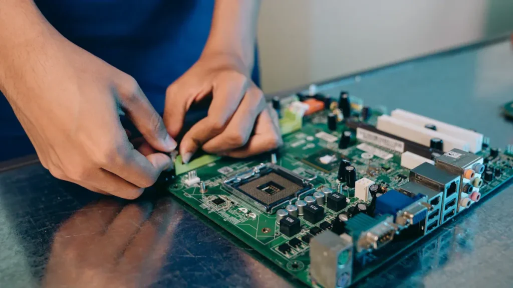
Choosing the right gold plating thickness for printed circuit boards affects how well your boards perform. You want the gold plating to last, but you also need to watch your costs. If you pick a thick gold PCB, you get more protection and better wear resistance. Too much gold, though, can raise the price without adding real value.
Key Takeaways
Pick the right gold plating thickness for your PCB’s use. This helps you save money and makes your PCB work better. Use thicker gold plating on parts that get used a lot, like edge connectors. This makes those parts last longer. Follow rules like IPC-4556 and ask your manufacturer about the best thickness. Use thick gold only where it really helps. This keeps costs down and quality high. Test and plan well so you do not have problems with gold that is too thin or too thick.
Gold Plating Factors
Application Needs
You should always start by thinking about how you will use your PCB. Some boards need to last a long time. Others need to handle many insertions and removals, like those with edge connectors. If you design a board for a computer or a server, you may need a hard gold pcb. This type of gold plating gives you a tough surface. It works well for parts that face a lot of wear and tear.
If your board only needs to carry signals and does not face much physical contact, you can choose a thinner gold plating. This saves money and still protects your board. You should also think about the environment. If your PCB will face moisture or chemicals, you need gold plating that offers good corrosion resistance.
Tip: Always match the gold plating thickness to the real-world use of your PCB. This helps you avoid over-engineering and keeps costs down.
Performance and Reliability
You want your PCB to work well and last a long time. Gold plating helps you reach both goals. A thicker layer of gold plating gives you better electrical contact. It also helps prevent problems like oxidation. If you use a hard gold pcb, you get even more durability. This is important for connectors that you plug in and out many times.
Some boards need to work in harsh places. In these cases, thicker gold plating can protect against damage. It also keeps the board working even if the surface gets scratched. You should always check if your design needs high reliability. If it does, do not pick the thinnest gold plating just to save money.
Cost and Manufacturing
You need to balance performance with cost. Gold is expensive. If you use too much, your project costs go up fast. You should only use thick gold plating where you really need it. For most boards, a standard thickness works well and keeps costs under control.
Manufacturers have limits on how thick or thin they can make the gold plating. If you ask for a very thick layer, it may slow down production or cause problems with the process. Some types of gold plating, like hard gold pcb, need special steps. This can add to the cost and time needed to make your board.
Checklist for Cost Control:
Use thick gold plating only on contact points.
Choose standard thickness for most surfaces.
Ask your manufacturer about their process limits.
You should also think about the environment. Using less gold helps save resources. It also makes your PCB more eco-friendly.
Why Thickness Matters
Electrical Performance
You want your PCB to carry signals without losing power. Gold plating helps you achieve this goal. Gold offers excellent electrical conductivity. This means your signals move quickly and do not face much resistance. If you use the right thickness, you get stable connections. Thin gold plating may wear away and cause weak spots. You should always check the thickness if your board handles important signals.
Note: A thicker layer of gold plating can help prevent signal loss in high-speed circuits.
Durability and Wear
You need your PCB to last through many uses. Gold plating protects the metal underneath from scratches and damage. If you use connectors that plug in and out often, thicker gold plating gives you more protection. This extra layer stands up to friction and keeps the contact points smooth. If you choose a thin layer, it may wear off quickly. You may see problems like poor connections or even failure.
Here is a quick comparison:
Thickness | Durability Level | Best Use Case |
|---|---|---|
Thin (0.03-0.05µm) | Low | Signal pads, low wear |
Standard (0.1µm) | Medium | General use |
Thick (0.76µm+) | High | Edge connectors, fingers |
Solderability
You want to make sure your PCB is easy to solder. Gold plating helps with this step. The right thickness lets solder flow smoothly and stick well. If the gold layer is too thin, the base metal may show through. This can cause poor solder joints. If the gold is too thick, it may make soldering harder or cost more than needed. You should also remember that gold plating gives your board strong corrosion resistance. This keeps your solder joints safe from moisture and chemicals.
Tip: Always match the gold plating thickness to your soldering process for the best results.
Typical Thickness Ranges
Standard Gold Plating Values
You need to know the standard values for gold plating on PCBs. Industry standards, like IPC-4556, help you choose the right thickness. Most gold plating types for PCBs fall between 0.03 microns and 1.0 micron. You often see 0.03–0.05 microns for signal pads. This thin layer works well for low-wear areas. For edge connectors and gold fingers, you usually need more protection. You should use 0.76 microns or more in these spots.
Here is a table to help you compare common thicknesses:
PCB Area | Typical Thickness (microns) | Use Case |
|---|---|---|
Signal Pads | 0.03–0.05 | Low wear, low cost |
General Contacts | 0.1 | Standard use |
Edge Connectors/Fingers | 0.76+ | High wear, frequent use |
Full Body Plating | 0.1–0.5 | Special applications |
Tip: Always check the IPC-4556 standard or ask your manufacturer for advice. This helps you match the gold plating thickness to your board’s needs.
Thick Gold PCB Applications
You use thick gold plating when your PCB faces heavy use or harsh conditions. A thick gold pcb gives you strong protection against wear and corrosion. You often see this in boards with edge connectors that get plugged in and out many times. Thick gold plating also helps in aerospace, military, and medical devices. These fields need high reliability and long life.
You should pick a thick gold pcb if your board must last for years or work in tough places. Thick gold plating can also help if your board faces lots of friction or needs to keep a perfect connection. You do not need thick gold plating everywhere. Use it only where you need extra strength.
When to use thick gold plating:
Edge connectors and gold fingers
Boards for aerospace or military
Medical devices
High-insertion connectors
Remember, thick gold plating costs more. Use it only where it adds real value.
Hard Gold PCB vs. Immersion Gold
You have two main choices for gold plating types: hard gold pcb and immersion gold. Each type has its own uses and thickness ranges.
A hard gold pcb uses electroplated gold. This process creates a tough, wear-resistant surface. You often see hard gold pcb on edge connectors and contact points. The thickness for hard gold pcb usually starts at 0.76 microns and can go higher. This makes it perfect for places that face lots of plugging and unplugging.
Immersion gold uses a chemical process. This type gives you a thinner, softer layer. You often see immersion gold on surface pads for soldering. The thickness for immersion gold usually stays between 0.03 and 0.1 microns. Immersion gold works well for fine-pitch components and places where you need good solderability.
Here is a quick comparison:
Feature | Hard Gold PCB | Immersion Gold |
|---|---|---|
Process | Electroplated | Chemical (ENIG) |
Typical Thickness | 0.76–1.0+ microns | 0.03–0.1 microns |
Wear Resistance | High | Low |
Solderability | Medium | High |
Best Use | Edge connectors | Solder pads |
Note: You should choose hard gold pcb for durability and immersion gold for easy soldering. Always match the gold plating type to your board’s real needs.
Thick Gold Plating Pros and Cons
Advantages
You get several benefits when you choose thick gold plating for your PCB. This type of gold plating gives you strong protection against wear and corrosion. You can trust your board to last longer, even in tough environments. Thick gold pcb surfaces keep their smooth finish, which helps with reliable connections. You also see fewer problems with oxidation. This means your signals stay clear and strong.
Longer lifespan for contact points
Better resistance to scratches and friction
Improved performance in harsh conditions
Tip: Thick gold plating works well for connectors that face many insertions and removals.
Drawbacks
You should also know the downsides of thick gold plating. The main issue is cost. Gold is expensive, so using more of it raises your project budget. Thick gold pcb designs may also take longer to manufacture. Some processes become harder with extra gold, which can slow down production. If you use thick gold plating where you do not need it, you waste resources.
Drawback | Impact |
|---|---|
Higher cost | Increases total project price |
Longer production time | Slower delivery |
Resource waste | Less eco-friendly |
When to Use Thick Gold PCB
You should pick a thick gold pcb when your board faces heavy use or needs to last for years. This choice makes sense for edge connectors, gold fingers, and boards in aerospace or medical fields. If your design needs high reliability and strong resistance to wear, thick gold plating is the best option. You do not need thick gold pcb everywhere. Use it only where it adds real value.
Note: Always match the gold plating thickness to your board’s real-world needs for the best results.
Selection Guide
Step-by-Step Checklist
You can choose the right gold plating thickness by following a simple checklist. This helps you make smart decisions and avoid mistakes.
Identify the PCB’s Purpose
Ask yourself what the board will do. Will it face lots of plugging and unplugging? Does it need to last for many years?Check the Contact Points
Look at the areas that will get the most use. Edge connectors and gold fingers often need thicker gold.Review Environmental Needs
Think about where the PCB will work. Will it face moisture, chemicals, or high temperatures? Tough environments need more protection.Select the Gold Type
Decide if you need hard gold or immersion gold. Hard gold works best for wear resistance. Immersion gold is good for solder pads.Match to Industry Standards
Use standards like IPC-4556 as a guide. These standards show common thickness values for different uses.Balance Cost and Performance
Choose the lowest thickness that still meets your needs. This saves money and resources.
Tip: Always talk to your PCB manufacturer. They can help you pick the right thickness for your design.
Risk Mitigation
You can avoid problems by planning ahead. Here are some ways to reduce risks:
Test Prototypes:
Build a sample board first. Check if the gold thickness works well in real use.Monitor Wear Points:
Watch for signs of wear on connectors and pads. If you see problems, adjust the thickness in your next design.Document Choices:
Write down why you picked a certain thickness. This helps you and your team remember the reasons later.
Risk | How to Avoid It |
|---|---|
Too thin gold | Follow standards, test samples |
Too thick gold | Review costs, use only where needed |
Wrong gold type | Match type to application |
🛡️ Note: Careful planning and testing help you get the best results from your gold-plated PCBs.
Choosing the right gold plating thickness helps your PCB last longer and work better. You should always match the thickness to your board’s job and reliability needs.
Check industry standards like IPC-4556.
Talk to your PCB manufacturer for advice.
Use thick gold only where needed.
For more details, look up IPC standards or visit trusted PCB manufacturing websites. Learning more helps you make smart choices for your next project.
FAQ
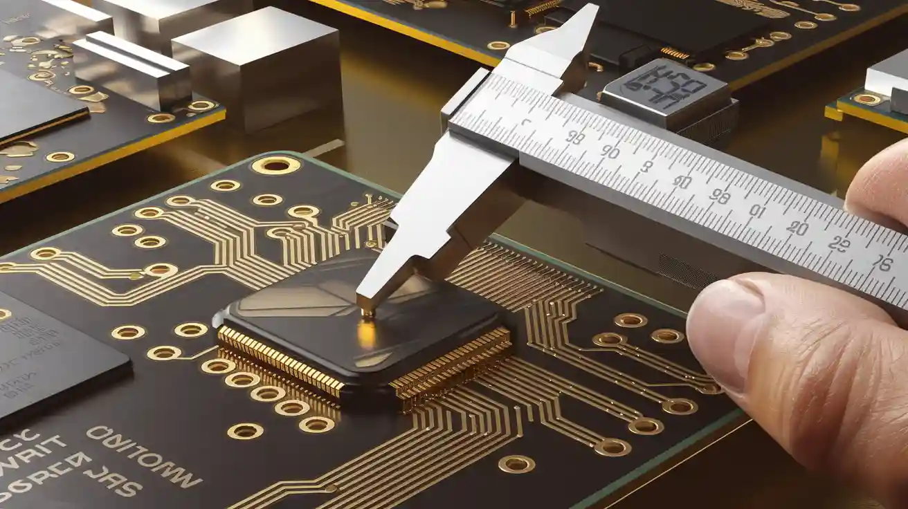
How do you measure gold plating thickness on a PCB?
You can measure gold plating thickness using X-ray fluorescence (XRF) tools. These tools give quick and accurate results. Ask your PCB manufacturer for a thickness report if you need proof.
What happens if you use too thin gold plating?
Thin gold plating can wear off fast. You may see poor connections or corrosion. Your PCB might fail sooner than expected. Always check the minimum thickness for your application.
Can you use thick gold plating everywhere on a PCB?
You should not use thick gold everywhere. Thick gold costs more and wastes resources. Use it only on high-wear areas like edge connectors or gold fingers.
Does gold plating affect soldering?
Yes, gold plating helps solder stick to pads. If the gold is too thin, soldering may become hard. If the gold is too thick, it can increase costs. Always match the thickness to your soldering needs.