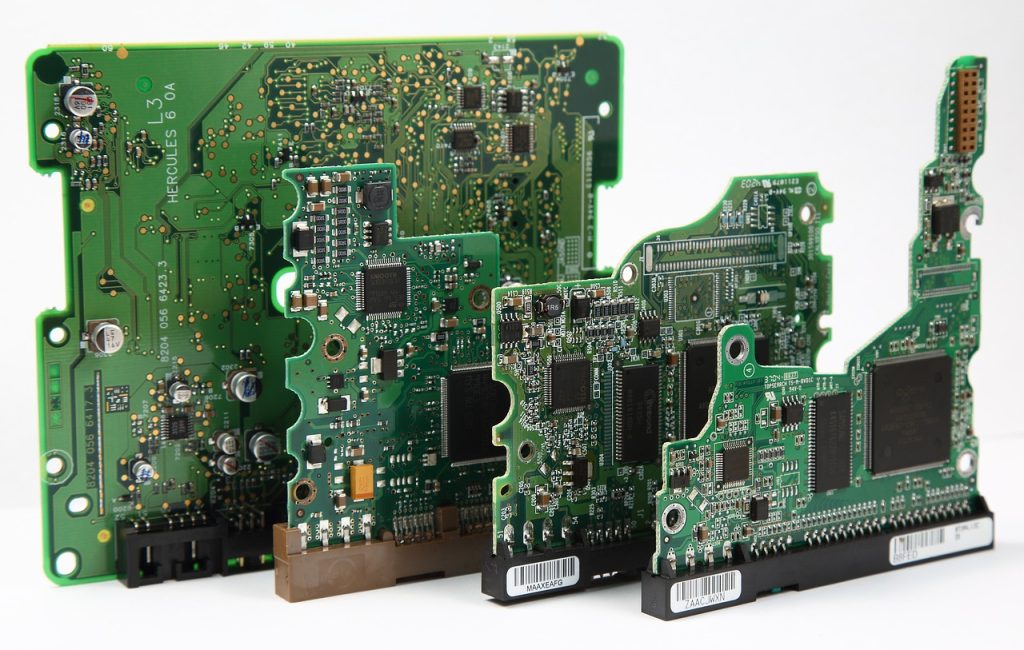
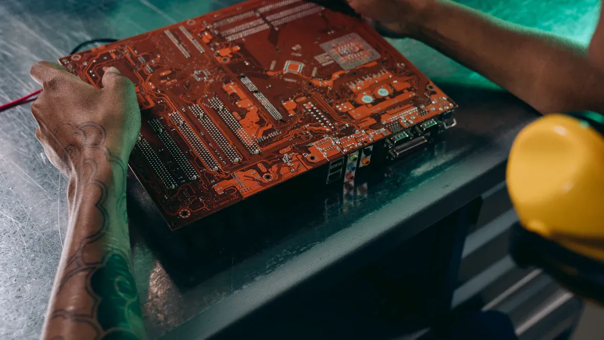
Smart phone circuit boards are the heart of every smart phone. These boards link and control all main parts, making your phone work smoothly. Their design and manufacturing require care and creativity to meet today’s tech needs.
The process starts by planning a layout that accommodates key parts like processors and memory chips. Creating smart phone circuit boards involves selecting materials, constructing the board, and adding components. Copying, often done through reverse engineering, raises moral and legal issues. For instance, studies show that better designs and recycling smart phone circuit boards can significantly benefit the environment. Additionally, using eco-friendly materials in production can lower costs and mitigate the effects of global warming.
Good practices and smart methods keep smart phone circuit boards functional, sustainable, and innovative.
Key Takeaways
Smartphone circuit boards link and control phone parts for smooth use.
Making a PCB needs good planning, picking materials, and smart layouts.
Building includes steps like preparing materials, assembly, and strict testing.
Copying PCBs by reverse engineering can be illegal and unfair.
The PCB industry is growing with green materials and new designs.
Design of Smart Phone Circuit Boards
Overview of Mobile Phone PCB Design
A mobile phone pcb is like the backbone of a smartphone. It connects important parts so they work well together. The design focuses on making it functional, small, and efficient. Engineers plan where processors, memory chips, and other parts go for better performance and space-saving.
New materials are improving mobile phone pcb designs. For example:
Stiff laminates and smooth copper help devices last longer.
Fast applications need careful control of dielectric constant (Dk) and dissipation factor (Df) to avoid signal problems.
Tests like thermal cycle testing check if the pcb can handle tough conditions.
High-end pcb demand shows how important innovation is. The market for these pcbs, worth USD 69.13 billion in 2023, may grow 7.6% yearly, reaching USD 115.31 billion by 2031.
Tools and Software for Designing Printed Circuit Boards
Making a pcb needs special tools and software. These tools let you see, test, and improve your design before production. Programs like Altium Designer, KiCad, and Eagle help with schematics, layouts, and 3D views.
The pcb software market is growing fast due to 5G, IoT, and AI. In 2022, it was worth USD 2.5 billion and may grow 6.4% yearly until 2032. By 2025, it could reach USD 3.17 billion, driven by demand from electronics and telecom industries.
Key Components and Layout Considerations
Designing a mobile phone pcb means thinking about key parts. These include processors, memory, power units, and wireless chips. Each part must be placed carefully for good signal flow and heat control.
The layout needs proper trace routing, layer stacking, and grounding. For fast applications, controlling impedance and reducing electromagnetic interference (EMI) are vital. Engineers use simulation tools to test these during design.
Tip: Focus on reliability and performance when designing a pcb. Tests like Conductive Anodic Filament (CAF) testing can find weak spots early.
Challenges in Designing Smart Phone Circuit Boards
Creating smartphone circuit boards is not easy. As technology grows, designers must make PCBs that handle new features like 5G and sharp displays. These needs make design and material choices harder.
Using advanced materials is a big challenge. High-quality PCBs often need polyimide, which lasts longer but costs more. Also, thinner and lighter phones make designs tricky. Designers must fit everything in small spaces while keeping it functional. This can raise costs and take more time to produce.
Note: Small companies find it hard to compete with big ones because they have fewer resources.
Following rules adds more challenges. Environmental laws require eco-friendly materials, which can be expensive. Testing for quality is also important. Tests like thermal cycle checks and impedance control are needed for fast devices but increase costs.
Fast-changing technology adds pressure. Designers must update their work often to match trends without spending too much. Adding new tech like AI and IoT makes this even harder.
Main challenges in PCB design are:
Adding advanced features like 5G and sharp displays.
Handling higher costs from better materials and testing.
Making small designs work well in thin devices.
Following strict environmental rules.
Keeping up with fast tech changes.
Making smartphone PCBs needs creativity and accuracy. Solving these problems helps meet modern tech needs.
Manufacturing Process of Mobile Phone PCBs
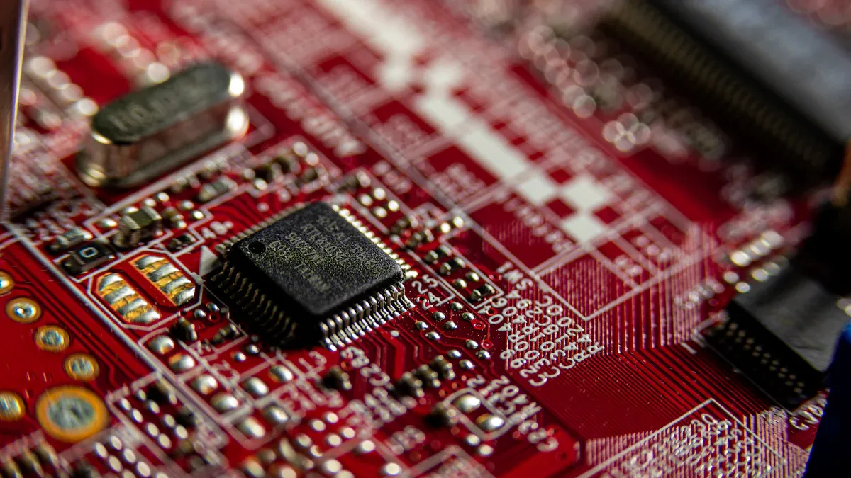
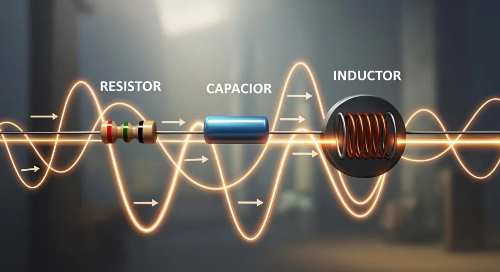
Material Selection for Printed Circuit Boards
Picking the right materials is very important for making a PCB. The materials affect how well the PCB works, lasts, and is made. For instance, thermal conductivity helps spread heat, and the coefficient of thermal expansion (CTE) stops damage from temperature changes.
Property | Description |
|---|---|
Thermal conductivity (K) | Shows how well heat moves, measured in W/m °C. |
Coefficient of Thermal Expansion (CTE) | Shows how much a material grows with heat, in ppm/°C. |
Dielectric constant (Er or Dk) | Impacts signal quality; values range from 2.5 to 4.5. |
Loss tangent (tanδ or Df) | Lower values mean less signal loss, great for fast signals. |
Moisture absorption | Shows how much water it absorbs, usually 0.01% to 0.20%. |
For low GHz uses, FR-4 is often used. For faster signals, advanced materials like Isola I-Tera MT40 are better. Always pick materials with low water absorption and strong CAF resistance for better performance.
Steps in PCB Fabrication
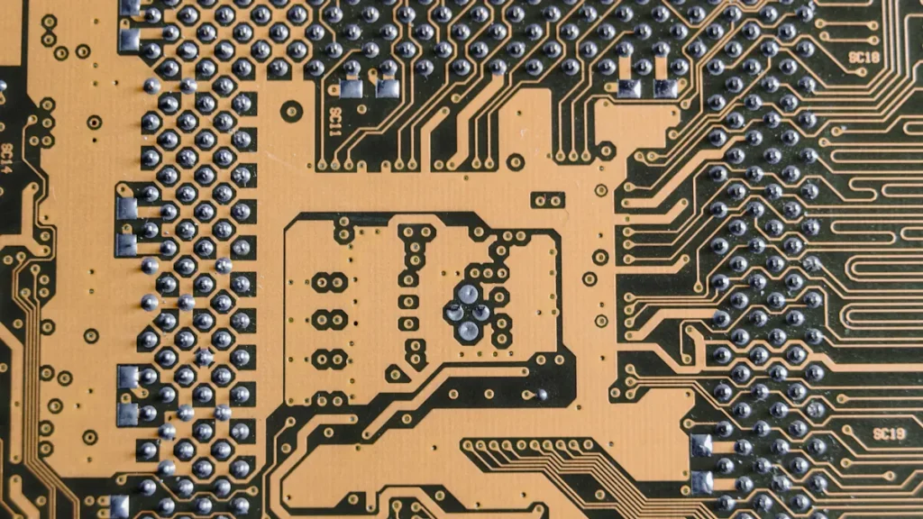
Making a PCB involves many careful steps. First, start with a fiberglass base covered in copper. Then, remove some copper to form the circuit paths. These paths carry electrical signals.
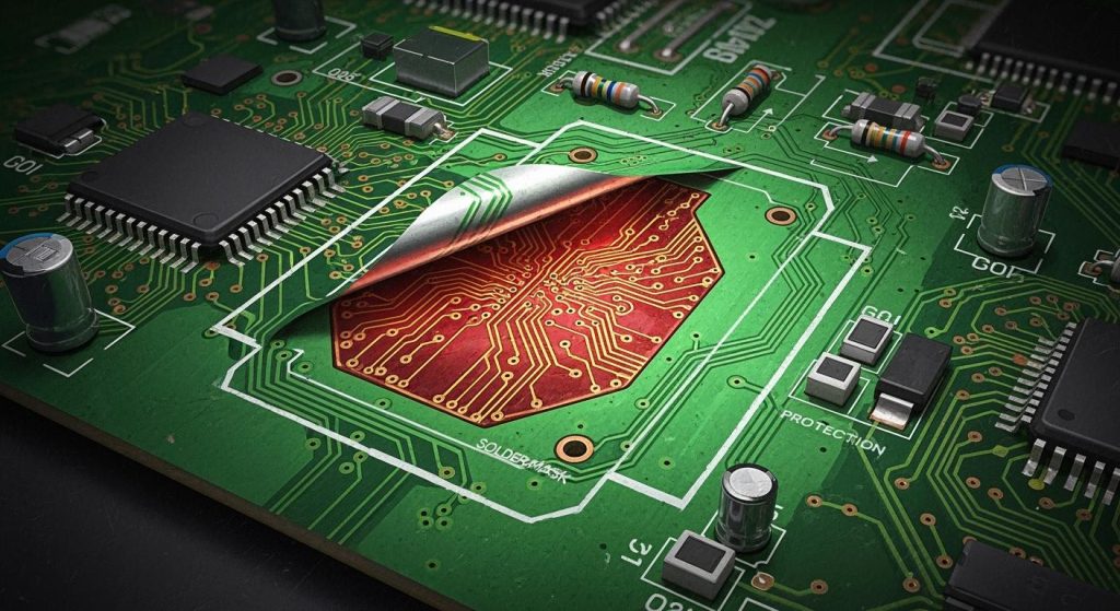
Next, add a solder mask to protect the circuits. Only areas for parts stay uncovered. After that, drill holes for vias and part leads. Finally, coat the holes and add a finish to help with soldering.
Good planning is key for smooth PCB production. Design mistakes can cause delays and cost more. Smaller parts make it harder, needing advanced methods to keep quality high.
Assembly and Integration of Components
After making the PCB, the next step is assembly. This means adding and soldering parts like processors and memory chips. Surface Mount Technology (SMT) is the main method. It places parts directly on the PCB, saving space and making production easier.
Once assembled, integration ensures all parts work together well. Testing is very important here. You need to check for electrical flow, signal quality, and heat control. Careful steps ensure good results, especially as phones get more advanced.
Tip: Test your PCB carefully to avoid problems later.
Quality Checks and Testing in PCB Production
Testing and quality checks are very important for a pcb. These steps find problems, boost performance, and keep high standards. Careful testing ensures the pcb works well in modern smartphones.
Common Testing Techniques
Manufacturers use different tests to check a pcb. Each test looks at specific parts of its quality and function. Here’s a list of common tests:
Test | What It Checks | Criteria |
|---|---|---|
Visual and X-ray inspection | Finds dirt, cracks, or damage in layers. | Pass/fail |
Peel test | Tests how strong the layers stick together. | Pass/fail + specific value |
Solder pot and float tests | Checks if holes can hold solder properly. | Pass/fail |
Automated optical inspection | Finds mistakes like missing or bad solder. | Pass/fail |
These tests make sure the pcb can handle smartphone needs. For example, the peel test checks layer strength, and optical inspection finds assembly mistakes.
Important Quality Measures
Manufacturers track key measures to check quality. These measures show how well the process works and where to improve. Some key measures are:
First Pass Yield (FPY): Shows how many pcbs pass tests the first time.
Defect Rate: Tracks the percentage of pcbs with problems.
Return Rate: Measures how many pcbs are sent back by users.
Failure Rate: Checks how often pcbs stop working during use.
Watching these measures helps find problems and fix them. For instance, a high defect rate might mean issues with materials or assembly.
Tip: Testing often and tracking results can save time and cut costs.
Copying of Smart Phone Circuit Boards
Methods of PCB Cloning and Reverse Engineering
Copying a mobile phone pcb uses a method called reverse engineering. This process helps recreate the design and function of a pcb. First, check how accessible the board is. Then, list all parts and make a bill of materials (BOM). If the board has a protective coating, remove it carefully. Next, collect datasheets and technical details for the parts. Finally, record each step using tools like Microsoft Visio. These steps help you copy the pcb correctly.
Reverse engineering needs special tools and software. For example, X-ray machines show internal layers, and schematic tools help rebuild the circuit. This process takes skill and accuracy.
Ethical and Legal Implications of Copying
Copying a pcb without permission is both unethical and illegal. It breaks intellectual property laws, which protect the creator’s work. This can lead to lawsuits and fines. Always get permission or a license before copying a design.
Ethically, copying discourages innovation. Duplicating a pcb without adding new ideas hurts creativity in the industry. Also, low-quality copies can fail, putting users at risk and damaging trust.
Note: Follow intellectual property laws and use ethical practices in your work.
Impact of PCB Copying on the Smartphone Industry
Copying pcbs affects the smartphone industry in big ways. It lowers costs, making phones cheaper. But it also creates unfair competition. Original makers spend a lot on research, while counterfeiters skip these costs.
Copied pcbs often use poor materials, causing devices to fail. This hurts consumer trust and damages the industry’s reputation. Copying also slows innovation. Companies may avoid creating new tech if they fear it will be copied.
To stop this, manufacturers use unique identifiers on their pcbs. These help prevent copying and protect intellectual property.
Strategies to Stop Unauthorized PCB Copying
Stopping others from copying a pcb is very important. It helps protect your ideas and keeps trust in the smartphone industry. Here are some ways to keep your designs safe:
Add Encryption and Security Features
Use encryption to protect your pcb design files. This makes it harder for others to steal them. Add unique codes or identifiers to track and confirm your pcb‘s authenticity.Use Protective Coatings and Layers
Cover your pcb with special coatings to block reverse engineering. Tamper-proof layers can hide the design, making it tough for others to access.Control Access to Design Files
Limit who can see your pcb design files. Store them on secure servers with passwords. Share only with trusted people or companies to avoid leaks.Get a Patent for Your PCB
Patents give legal protection for your pcb. They stop others from copying your design without permission. Patents also warn counterfeiters of legal risks.Watch for Counterfeit Products
Check the market often for fake copies of your pcb. If you find any, act quickly. You can take legal steps or improve security to stop future copying.
Tip: Using several methods together works best to protect your pcb designs.
By following these steps, you can secure your pcb designs and support a fair, creative industry.
Smartphone circuit boards are key to today’s technology. Designing a pcb needs smart planning, picking the right materials, and good layouts. Making them takes careful steps, from preparing materials to putting parts together and testing. Copying can help learning but brings ethical and legal problems.
The pcb industry needs new ideas and fair practices. Companies now use eco-friendly materials like lead-free solder and safe laminates to follow green rules. Big companies like Apple plan to use only recycled or renewable materials by 2030, setting a good example.
The future of smartphone pcb looks exciting:
The market for mobile phone pcb may grow over 10% yearly until 2027, thanks to high-speed uses.
Green efforts are changing how pcb are made to meet rules like RoHS.
There are still challenges, but the industry is growing fast.
Metric | Value |
|---|---|
Market size in 2023 | USD 84.4 Billion |
Market size in 2032 | USD 139.63 Billion |
Growth Rate | 5.7% |
Annual smartphone shipments | 1.3 billion units |
As people want better circuit tech, more cool designs and methods will come. By staying creative and fair, the pcb industry will keep growing strong.
FAQ
What is a PCB, and why is it important in smartphones?
A PCB, or printed circuit board, is like a smartphone’s backbone. It links all the electronic parts and helps them work together. Without it, your smartphone wouldn’t work at all.
How do you ensure the quality of a PCB during manufacturing?
Manufacturers check PCBs using tests like visual checks and peel tests. They also use automated tools to find defects and test soldering. These steps make sure the PCB works well and meets standards.
Can you copy a PCB design legally?
You can only copy a PCB design if you have permission. Doing it without approval breaks laws and stops new ideas. Always follow rules and act responsibly with PCB designs.
What materials are commonly used in PCB manufacturing?
Materials like FR-4 and polyimide are often used for PCBs. These materials are strong, handle heat well, and keep signals clear. Picking the right material helps the PCB work better in smartphones.
How does PCB design impact smartphone performance?
PCB design affects how parts communicate and handle heat. A good design makes signals faster and reduces problems. Engineers carefully plan layouts and pick materials to improve smartphone performance.