PCB manufacturing uses many ways to check quality in printed circuit boards. The inspection process has visual checks, electrical testing, and automatic laser measurement. PCB inspection happens at different times during production. Bare board inspection finds problems before assembly. Assembled PCB inspection looks at solder joints and where parts are placed. These steps help stop faults in pcbs and make them work better. Inspection methods are very important in every part of making both bare boards and assembled pcbs.
Key Takeaways
Early inspection of bare PCBs uses electrical tests and laser measurement. This helps find problems before assembly. It saves time and money.
Automated visual inspections with AI spot tiny defects quickly. They do this better than manual checks. This improves quality and cuts down on waste.
Assembly inspections like AOI, SPI, and X-ray work together. They find surface and hidden problems. This makes sure solder joints are strong. It also checks that parts are in the right place.
Electrical tests like in-circuit and flying probe testing check if PCBs work right. They make sure PCBs meet industry standards before shipping.
Final inspections and good documentation protect product quality. They help with compliance. They also help manufacturers make better PCB designs in the future.
PCB Manufacturing Inspection
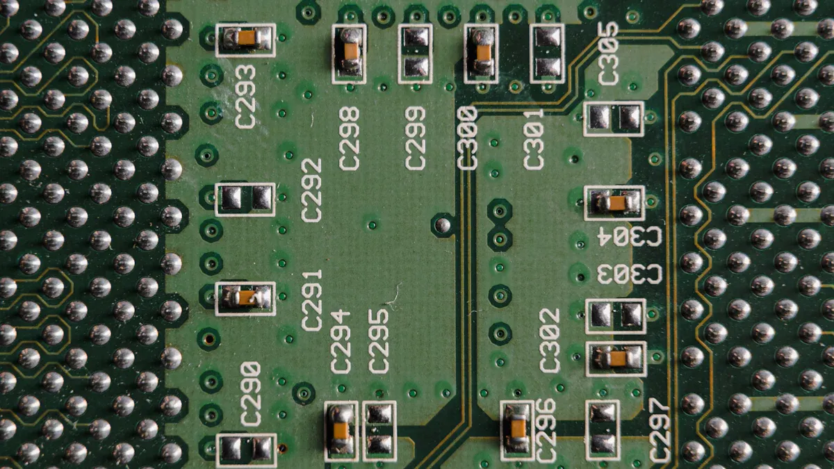
Bare Board Testing
Bare board testing checks printed circuit boards before adding parts. This step helps find problems early in the pcb manufacturing process. Electrical probes are used to look for open circuits and short circuits. These tests make sure every trace and via on the pcb works right. If a problem is found now, the manufacturer can fix it before assembly. This saves both time and money during production.
Bare board testing also checks the board’s size and shape. Manufacturers use special tools to measure the board and see if it matches the design. This step stops problems from happening later in assembly. When defects are found early, manufacturers avoid expensive repairs and delays.
Visual Inspection
Visual inspection is one of the oldest and easiest ways to check pcbs. Workers or machines look at the bare board to spot visible problems. These problems include scratches, missing pads, or extra copper. Manual visual inspection works well for simple pcbs, but it can miss small or hidden issues. As pcb designs get more complex, manual inspection does not work as well.
Note: Manual visual inspection often misses many problems and is slow. It is not good enough for making lots of pcbs. Machine vision-based inspection can check many pcbs each minute and finds tiny defects as small as 0.01 mm.
The market for visual inspection tools is growing quickly. In 2024, the market size was USD 1.2 billion. Experts think it will grow to USD 2.5 billion by 2033. This growth happens because people want better electronics and more complex printed circuit boards. New technology like AI and machine learning helps machines find problems more easily. These new tools help save time and money, and they also help reduce electronic waste.
Metric/Aspect | Details |
|---|---|
Market Size (2024) | USD 1.2 Billion |
Projected Market Size (2033) | USD 2.5 Billion |
CAGR (2026-2033) | 9.2% |
Key Market Drivers | Demand for reliable electronics, PCB complexity, automation, growth in key sectors |
Technological Trends | AI, machine learning, smart manufacturing, IoT integration |
Importance | Ensures quality, reduces costs and waste, supports reliability |
Automatic Laser Measurement
Automatic laser measurement uses lasers to check the size and shape of pcbs. This method gives very accurate results. Good laser tools can measure with an error as small as 0.0005 inch (0.0127 mm). Some laser systems use cameras and Bluetooth to send data fast. These tools can also measure area and volume, which helps check copper thickness or hole depth.
Manufacturers use automatic laser measurement to make sure each pcb matches the design. This step is important because even small mistakes can cause problems in the final product. Laser measurement is faster and more accurate than checking by hand. It also helps with fully automatic inspection during production.
Laser measurement devices can be accurate up to 1/16 inch at 400 feet.
Some systems use deep learning to measure coating sizes with over 98% accuracy.
High-accuracy laser interferometers can reach 2-3 micro-inch precision.
Automatic laser measurement helps manufacturers find problems early. This cuts down on waste and makes printed circuit boards more reliable.
Assembly Inspection Methods
After putting parts on the pcb, manufacturers check for problems. They use different inspection methods to find defects. These checks look for things like bad soldering, missing parts, or parts in the wrong place. Good inspection at this step makes pcbs work better and last longer.
Manual Visual Inspection
Manual visual inspection means trained workers look at each pcb. They search for problems they can see, like missing parts or bad solder joints. This method is good for small batches or simple boards. Sometimes, workers find issues that machines do not see. This is helpful for custom or special products.
But manual inspection is not perfect. People can get tired or make mistakes. Studies show it finds most defects, but not all. Inspectors can check about 50 to 100 items every hour. The results depend on how skilled each worker is. This can make the results different each time.
Feature | Manual Inspection | Automated Inspection |
|---|---|---|
Speed | 50-100 items/hour | 2,000-3,000 items/hour |
Accuracy | 85%-95% | Up to 99.9% |
Labor Dependency | High | Minimal |
Scalability | Difficult | Easily scalable |
Flexibility | High for custom jobs | Best for standardized products |
Manual inspection is best for prototypes or special designs. For big jobs, automated inspection is faster and more accurate.
Automated Optical Inspection (AOI)
Automated optical inspection uses cameras to check pcbs after assembly. AOI systems scan each board and compare it to a good image. They find problems like missing parts, wrong parts, or solder bridges. AOI works much faster than people and gives steady results.
Modern AOI uses artificial intelligence and machine learning. These systems can check 2,000 to 3,000 items every hour. They can be almost 99.9% accurate. In one study, AI models found over 98% of defects. This helps manufacturers fix problems early and waste less.
Study / Method | Dataset Details | Metrics Reported | Results Summary |
|---|---|---|---|
Nahar and Phadke (2019) | 103 PCBA samples, 134 defects | Detection accuracy | 91.1% detection accuracy without defect class discrimination |
Bhattacharya and Cloutier (2022) | 1,386 images, 6 defect classes | Mean accuracy, False positive rate | Mean accuracy of 98.3%, false positive rate under 5% |
T-YOLOv5 Model (Improved YOLOv5) | PCB dataset (unspecified size) | Accuracy, Recall, mAP (IoU=0.5), Statistical significance (t-values, p-values) | Accuracy: 98.37%, Recall: 99.24%, mAP: 99.15%; t-values > 1.96, p-values < 0.001 |
Automated optical inspection cuts down on mistakes and boosts how many boards can be checked. About 72% of companies using it see a 50% jump in output. AOI also keeps records of each pcb’s inspection.
Solder Paste Inspection (SPI)
Solder paste inspection checks the solder paste before adding parts. SPI uses 3D images to measure how much paste is on the board. Good solder paste is needed for strong joints and good connections.
SPI finds problems like not enough paste, too much paste, or paste in the wrong spot. These issues can cause open circuits, shorts, or weak joints. Automated SPI works fast and gives detailed reports. It helps fix printing problems before they spread.
SPI is an important step in pcb assembly. It stops many common defects and helps more boards pass the first test. By finding problems early, SPI lowers the need for rework and cuts waste.
X-Ray Inspection
X-ray inspection looks inside pcbs to find hidden problems. This is important for boards with tricky layouts or parts like BGAs. X-ray can find voids, solder bridges, and cracks that other checks miss.
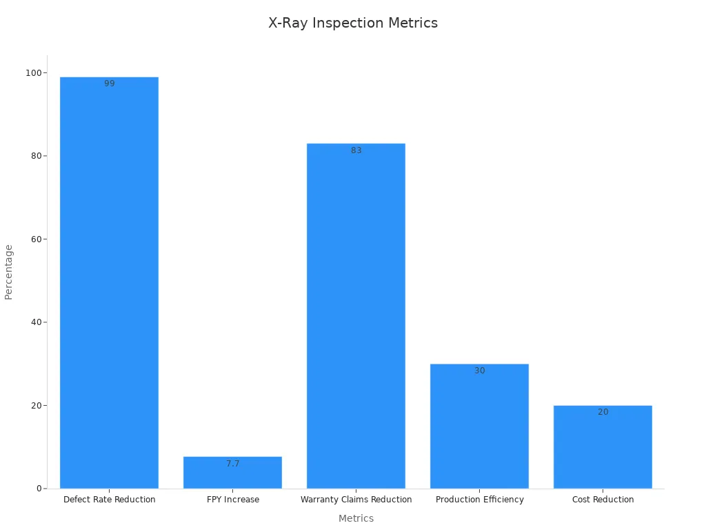
Advanced x-ray uses micro-CT to make 3D images of the pcb. These systems can spot tiny defects smaller than 0.015 mm. Automated x-ray can cut defect rates by up to 99%. It can raise first pass yield from 92% to 99.7% in car electronics. Manufacturers can also save up to 20% in costs and make 30% more boards.
X-ray inspection is great for finding hidden faults. It helps make high-quality pcbs and meet tough industry rules.
Tip: Using AOI, SPI, and x-ray together works best. Each method finds different problems, so the inspection is more complete.
Typical Defects Detected During Assembly Inspection
Assembly inspection finds many types of defects, such as:
Solder bridges and open joints
Parts in the wrong place or missing
Tombstoning (parts standing on end)
Not enough or too much solder paste
Voids and cracks in solder joints
Bent or broken leads
These steps make sure pcbs are good before moving on. Automated inspection, especially with AI, keeps getting better at finding defects and making more boards.
Electrical Testing
Electrical testing plays a key role in PCB inspection. It checks if each board works as designed before it leaves the factory. Manufacturers use several testing methods to find faults that visual or x-ray inspection might miss. These methods help ensure that every pcb meets strict industry standards and works in real-world conditions.
In-Circuit Testing (ICT)
In-circuit testing uses a bed-of-nails fixture to check each component on the pcb. It finds problems like open circuits, shorts, and wrong parts. ICT can test a board with 300 parts in just 3-4 seconds. This speed makes it perfect for mass production. The method covers 95% to 98% of possible faults, making it one of the most reliable inspection steps.
Metric | Value | Description |
|---|---|---|
Fault Coverage | 95% – 98% | High detection rate for opens, shorts, and errors |
Testing Time | 3-4 seconds per 300 parts | Fast for large batches |
Flying Probe Testing
Flying probe testing uses moving probes to touch test points on the pcb. It does not need a custom fixture, so it works well for prototypes and small batches. This method covers 80% to 90% of faults. It acts like an automated multimeter, giving detailed reports for each board. Flying probe testing helps engineers debug new designs and find problems early.
Test Method | Typical Test Coverage |
|---|---|
Flying Probe | 80-90% |
Bed of Nails | 90-95% |
In-Circuit Test | 95-98% |
Boundary Scan | 95-99% |
Boundary Scan Testing
Boundary scan testing checks connections inside chips using special test circuits. It works well for dense or complex pcb assemblies where other inspection tools cannot reach. This method gives fast results and lowers setup costs. Boundary scan can find faults down to the pin level. It is best for boards with JTAG-compliant chips.
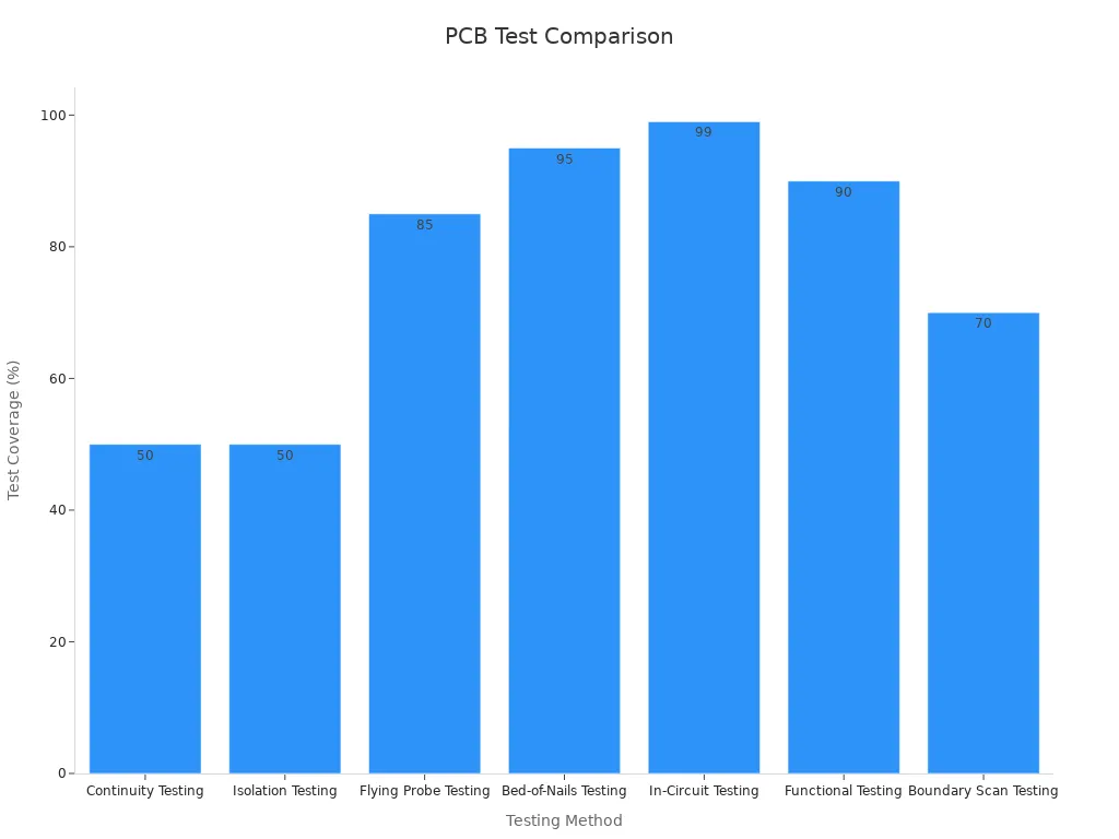
Functional Testing
Functional testing powers up the pcb and checks if it works in real conditions. It loads firmware and tests logic, input/output, and system stability. This step finds up to 70% of performance problems that other inspection steps might miss. Functional testing is the last check before shipping, making sure each board meets customer needs.
Industry standards like IPC-SM 785, IPC 9701, MIL-STD 202, and JEDEC guide all these inspection and testing steps.
Testing tools include flying probe testers, fixtures, and time domain reflectometers.
These methods ensure that each pcb is safe, reliable, and ready for use in fields like medical and aerospace.
Reliability and Stress Testing
Burn-in Testing
Burn-in testing helps find weak PCBs before shipping. The PCB is run at high heat and voltage for a set time. This makes early failures happen in the factory, not later. Engineers use burn-in to see how long a PCB can last under stress. Studies show that using test data and computer models helps predict PCB life. These methods help engineers make better designs and longer-lasting boards. Burn-in testing is important for making sure only good PCBs move forward.
Environmental Stress
Environmental stress testing checks how PCBs handle real-world use. Engineers use heat, cold, shaking, and wet air to test boards. This testing finds problems like cracks or changes in resistance. Researchers use the Interconnect Stress Test (IST) to speed up aging and find weak spots. Statistical models, like the Norris-Landzberg equation, help measure how changes affect reliability. Testing with different stresses shows what makes PCBs last longer. These tests help makers predict failures and improve quality.
Environmental stress testing finds hidden failures, like microvia problems.
Statistical models and sample size checks show if reliability gets better.
Fast tests copy real-life use and help predict long-term failures.
Solderability and Contamination
Solderability and contamination testing checks if PCBs can make strong, clean joints. Bad solderability causes weak connections and early failures. Engineers use different tests to see how well solder sticks to pads and leads.
Test Name | Quantitative Metrics | Description |
|---|---|---|
Wetting Balance (Meniscograph) | Wetting force, Wetting time | Measures how much force molten solder uses on pads over time, making a wetting curve. |
Surface Insulation Resistance (SIR) | Insulation resistance values | Checks for contamination by measuring resistance between conductors in controlled conditions. |
Dip and Look Test | Qualitative | Visual check of solder coverage; not a measured value. |
These tests help makers find and fix problems before assembly. By using wetting balance and SIR tests, they make sure each PCB meets high standards for quality and reliability.
Final PCB Inspection
Final Visual Checks
Final visual checks are the last step before shipping. Inspectors look at each board very carefully. They try to find any problems missed earlier. They look for scratches, missing parts, or bad solder joints. This step makes sure every board is good and meets what customers want.
Manufacturers use different ways to check boards at this stage. These ways include visual inspection, automated optical inspection, x-ray inspection, electrical testing, and sometimes cross-sectional analysis. Each way has something it does best. Visual inspection is fast and cheap but only finds surface problems. Automated optical inspection is good for big groups of boards and is very exact. X-ray inspection can see inside the board to find hidden issues. Electrical testing checks if the board works right. Cross-sectional analysis is destructive but shows the inside of the board.
Inspectors use industry standards like IPC-A-600 and IPC-6012. These rules say what counts as a problem and how to check quality. Final visual checks help lower the number of bad boards and make products better. They also give data to help make future boards even better.
Tip: Final inspection is the last chance to find problems before customers get the boards. Careful checking now protects the company’s name and stops expensive returns.
Documentation
Documentation is an important part of the last inspection step. It keeps track of every check and result from the inspection. Good records help manufacturers find and fix problems early. They also show that each board meets all the needed rules and standards.
Documentation helps follow rules and keeps customers happy.
It keeps notes about problems and how they were fixed.
It helps plan how to make boards in the future.
It gives a record for audits and keeps suppliers honest.
It helps control quality and lowers risk.
The process includes looking at design papers, checking materials, and writing down inspection results. Keeping good records makes sure only boards that pass all checks move on. Documentation is very important in fields like aerospace, cars, electronics, and medical devices. It helps companies follow strict rules and send out good products.
A good inspection and testing process helps make high-quality pcbs. Each way of checking, like looking by eye or using x-ray, finds problems early. This keeps printed circuit boards working well. Testing steps such as in-circuit and functional testing show if pcbs work in real life. Quality control tools like Statistical Process Control and Six Sigma help stop mistakes and make things better.
Visual, AOI, and x-ray inspection find problems before they get worse.
In-circuit and stress testing show pcbs can handle hard conditions.
Using data for quality control lowers mistakes and saves money.
These steps help pcbs pass tough rules for cars, planes, and other uses.
FAQ
What is the difference between AOI and X-ray inspection?
AOI uses cameras and light to check the board’s surface. It finds problems you can see, like missing parts or bad solder. X-ray inspection looks inside the PCB. It finds hidden problems, like cracks or empty spaces under parts. Both methods help make PCBs better, but they find different problems.
Why do manufacturers use both manual and automated inspections?
Manual inspection is good for small or special boards. Automated inspection checks many boards fast and very accurately. Using both ways helps find more problems and makes sure boards are high quality.
How does solder paste inspection (SPI) help in PCB assembly?
SPI checks how much solder paste is on the board and where it is. This step stops weak joints, open circuits, and shorts from happening. Good solder paste coverage makes connections stronger and more reliable.
What standards guide PCB inspection and testing?
Industry standards like IPC-A-600, IPC-6012, and JEDEC set rules for PCB quality. These rules tell makers what to check and how to measure problems. Following these rules keeps PCBs safe and reliable.