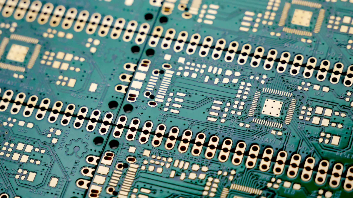
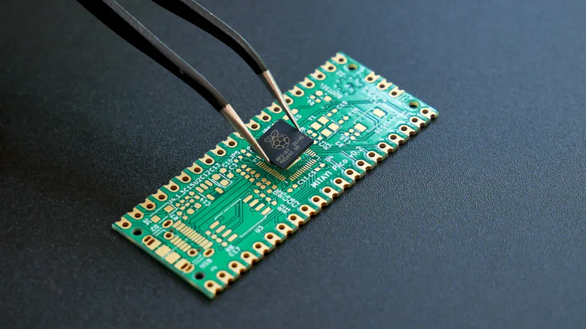
Printed circuit boards (PCBs) are important in modern electronics. A bare PCB is a plain board with no parts on it. It is the base for circuits and needs assembly to work. These boards are used where accuracy and dependability are key.
Zero PCBs, on the other hand, are great for testing ideas. They have no set connections, so they are good for experiments. As small gadgets like IoT devices and wearables grow, flexible boards are needed more. Zero PCBs help by being cheap and easy to design with.
Key Takeaways
Bare PCBs are the base for electronic circuits. They need to be built and tested to work well in things like cars and medical devices.
Zero PCBs are great for trying out ideas. Their open design lets you make custom connections, perfect for testing and creating new projects.
Testing bare PCBs is very important. It finds problems early, saves time and money, and makes sure the product works well.
Pick the right PCB for your project. Use bare PCBs for accurate work and making many copies. Use zero PCBs for learning and trying new things.
Zero PCBs are cheap for students and hobbyists. They let you change designs quickly and waste less during testing.
Bare PCBs: Characteristics and Structure
Key Features of Bare PCBs
Bare PCBs are the base of modern electronics. They are plain boards used to hold electronic parts. These boards are made carefully to ensure they work well. A bare PCB has layers of materials that help signals move smoothly.
Wildriver Technology used a special platform to study signal loss. This platform was made for Isola to test their new low-loss material, I-Tera® MT40.
Bare PCBs are tested to meet strict rules. For example, heat tests check how they handle temperature changes. Other tests check if they work in tough environments. These features make them important for cars, planes, and medical tools.
Components of a Bare PCB
A bare PCB has key parts that help it work:
Component | Description |
|---|---|
Substrate | Gives support and insulation, often made from FR4 material. |
Copper Traces | Create paths for signals, etched on the board for accuracy. |
Vias | Link layers in multi-layer boards, like through-hole or blind vias. |
These parts help the PCB handle complex designs and stay reliable. For example, copper traces carry signals, and vias connect layers.
Functionality of Bare PCBs
A bare PCB works by holding and linking electronic parts. You can test it in different ways to make sure it works:
Look for problems like misplaced parts or solder issues.
Check if parts are placed the right way.
Test if electrical paths are complete and not broken.
Make sure the power supply gives the right voltage.
Test how the PCB works in a full system.
These checks make sure the PCB works well and is ready for real-world use.
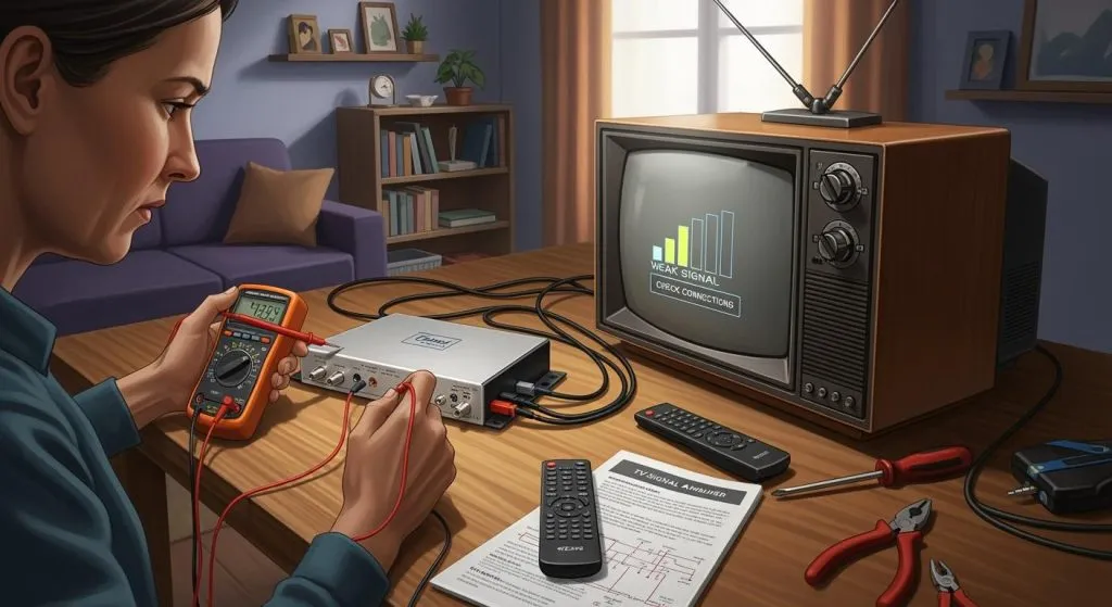
Testing Methods for Bare PCBs
Why Testing Bare Boards Matters
Testing makes sure a bare PCB works before adding parts. It helps find problems like broken paths or design mistakes. Testing is important to keep your circuit reliable. Without it, you might build a bad board. This could cause expensive fixes or failures in important devices like cars or medical tools.
Testing also checks if the board’s electrical parts are correct. It looks for shorts, open circuits, and proper connections. This step ensures the board can handle your design needs. Catching mistakes early saves time and money. It also improves the quality of your project.
Flying Probe Test: A Flexible Way to Test
The flying probe test is a handy way to check circuits. It uses moving probes to find shorts, open paths, or wrong resistance. This test doesn’t need a fixed setup, so it’s great for prototypes. You can test many things without turning on the board. This lowers the chance of damage.
This method is cheap and fast. For example, testing one board takes 1 to 3 minutes. The flying probe test is perfect when you need flexibility and low costs. It helps you fix your design before making many boards.
Fixture Test: Best for Large Production
The bed-of-nails test, or fixture test, is for making lots of boards. It uses a fixed setup with many probes to test the PCB. This method is faster and more exact than the flying probe test. It can test a board in 5 to 10 seconds, making it great for mass production.
In-circuit testing is another good choice for large production. It finds up to 90% of problems and reduces human mistakes. Though it needs a special setup, it’s fast and accurate. This makes it useful for making many boards.
Testing Method | Benefits | Time Needed |
|---|---|---|
Flying Prober | Cheap, no fixed tools, good for prototypes | 1 to 3 minutes |
Nail Bed Fixture | Fast, accurate, reusable tools, good for mass production | 5 to 10 seconds |
In-Circuit Testing | High problem detection (85%-90%), fewer human errors | Varies |
Picking the right test ensures your PCB is high-quality and reliable.
Zero PCBs: Features and Flexibility
Characteristics of Zero PCBs
Zero PCBs are special because they have no set paths. Think of them as blank boards for your circuit ideas. They have small holes in a grid pattern. You can add parts and connect them with wires or solder. This makes zero PCBs great for testing and trying out circuits.
Unlike bare PCBs, zero PCBs don’t have a fixed design. You choose how to link the parts, giving you full control. This is very helpful for prototypes or small projects.
Structure and Design of Zero PCBs
Zero PCBs are simple but useful. They are flat boards made of insulating material like fiberglass. The board has a grid of holes, each lined with copper. The copper helps make electrical connections between parts.
The design is easy to use. You can place parts anywhere and connect them with wires. This open design lets you try new ideas without limits.
Customization and Adaptability in Circuit Design
Zero PCBs let you customize your circuit as needed. You can change the layout easily, which is great for testing. For example, if you’re trying a new idea, you can adjust connections without starting over.
These boards are also very flexible. Whether it’s a simple LED circuit or a complex prototype, zero PCBs work well. This saves time and materials, especially in early project stages.
Tip: Use different colored wires to track your connections. This helps avoid mistakes and makes fixing problems easier.
Applications of Zero PCBs
Prototyping and Experimentation
Zero PCBs are great for testing new circuit ideas. They have a grid of holes with copper linings. This lets you make custom connections without a fixed design. You can try different setups and improve your design easily. Adding or removing parts is quick, so changes are simple. This hands-on method shows how your circuit works in real life.
For example, if you’re making an LED circuit, use a zero PCB. You can test where to place resistors and wires. This helps ensure your design works before making it permanent. By using zero PCBs, you learn more about circuits and get better at building them.
Cost-Effective Circuit Evaluation
Zero PCBs save money when testing circuits. They let you check your ideas early, avoiding costly mistakes. Fixing problems before production reduces waste and lowers costs. You don’t need expensive tools, which makes them affordable for small projects.
Advantage | Description |
|---|---|
Saves money | Cuts costs by reducing redesign and remanufacturing needs. |
Early testing | Lets you test ideas without spending too much. |
Less waste | Fixes problems early, saving time and materials. |
Zero PCBs are perfect for hobbyists, students, and small-scale projects. They are cheap and easy to use during the testing phase.
Common Use Cases for Zero PCBs
Zero PCBs are useful in many areas. Teachers use them to show students how circuits work. Hobbyists use them for DIY electronics projects. Engineers use them to test gadgets like IoT devices and wearables.
These boards are helpful when circuits need frequent changes. For example, if you’re building a sensor system, a zero PCB lets you try different setups. This flexibility ensures your final design works well.
Tip: Write labels for your parts and connections on the board. This keeps things organized and makes fixing problems faster.
Comparing Bare PCBs and Zero PCBs
Differences in Structure and Functionality
Bare PCBs and zero PCBs are built differently. A bare PCB is a plain board with fixed copper paths. These paths guide signals and connect parts accurately. Zero PCBs, however, have no fixed paths. They have a grid of holes with copper, letting you make custom links.
Their uses are also different. Bare PCBs are made for specific tasks and are great for mass production. They work well in devices needing high performance. Zero PCBs are flexible and let you test and change designs. This makes them ideal for experiments and prototypes.
Applications and Suitability for Various Projects
Each PCB type fits different projects. Bare PCBs are best for reliable and precise tasks, like in cars or medical tools. Their fixed design ensures they work the same every time. Zero PCBs are great for learning and testing ideas. They let you try things without sticking to one design.
For example, a bare PCB is perfect for a strong, efficient wearable device. A zero PCB is better for students learning circuits. It allows mistakes without wasting money. Your choice depends on how complex your project is and what you need it to do.
Choosing the Right PCB for Your Needs
Picking the right PCB means thinking about your project’s needs. Look at cost, design difficulty, and how many you’ll make. If saving money matters, zero PCBs are cheaper. If you need accuracy, bare PCBs are the way to go.
You can also use tools like charts to check quality. These tools help ensure your PCB works well. By matching your choice to your project’s goals, you save money and get the best results.
Knowing the difference between bare PCBs and zero PCBs helps. Bare PCBs are plain boards with copper paths and vias. They need assembly and testing to work properly. Zero PCBs have a grid of holes, making them great for testing ideas.
Testing bare PCBs is important to avoid big mistakes. It ensures they work well in important devices. Zero PCBs save time and money by allowing quick changes during design.
Type of PCB | Features | Uses |
|---|---|---|
Bare PCB | Plain boards with copper paths and vias, needing assembly and testing. | Best for making reliable circuits in large numbers. |
Zero PCB | Boards with holes and no fixed paths, very flexible for changes. | Great for testing and building custom circuits. |
Pick the PCB that fits your project. Bare PCBs are precise, while zero PCBs are flexible. Both are useful for different needs in electronics.
FAQ
What makes a bare PCB different from a zero PCB?
A bare PCB has fixed copper paths and needs assembly to work. A zero PCB has no set connections. You can design it freely for testing and experiments.
Can a zero PCB be used again for other projects?
Yes, you can reuse a zero PCB. Remove the parts and clean the board. This lets you use it for new designs, saving money on experiments.
Why is it important to test bare PCBs?
Testing checks if a bare PCB works before adding parts. It finds problems like broken paths early. This saves time, money, and improves reliability.
Are zero PCBs good for professional use?
Zero PCBs are great for testing and small projects. But for big, professional tasks, bare PCBs with fixed designs are better and more reliable.
How do you decide between a bare PCB and a zero PCB?
Think about your project’s needs. Use bare PCBs for precise, large-scale tasks. Pick zero PCBs for flexible designs and testing. Cost and purpose help you decide.