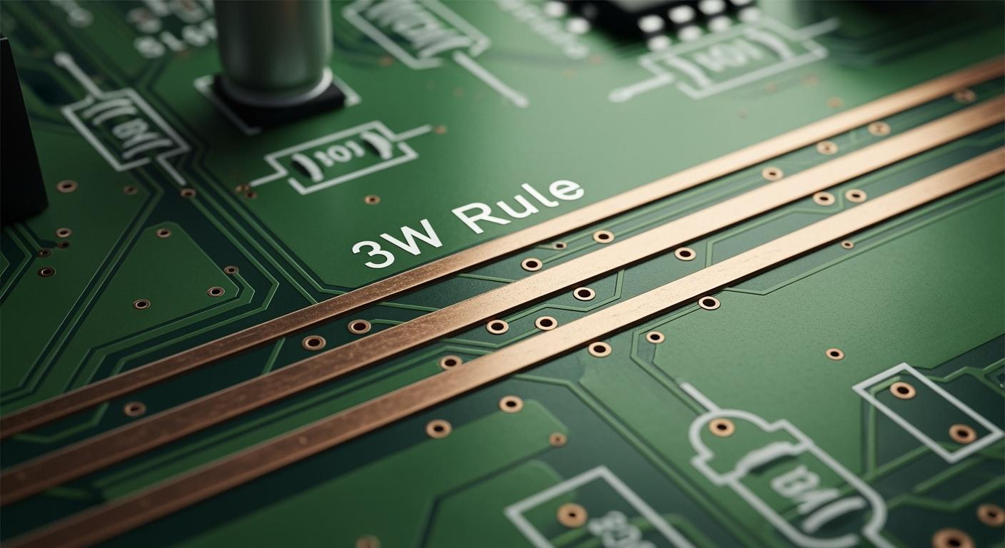
You use the 3W rule in pcb design to keep traces apart. The space should be at least three times the width of each trace. This rule is simple and helps stop crosstalk. It also keeps signals clear and strong. Think about talking to a friend in a loud room. If you have more space, it is easier to hear each other. Crosstalk is when signals mix and cause mistakes. The table below shows how the 3W rule helps stop these problems.
Parameter | Guideline for Critical Signals | Impact of Non-Compliance |
|---|---|---|
Trace Spacing | 3W Rule: Space traces at least 3x their width | More inductive and capacitive coupling, which can cause data errors. |
If you are new to pcb design or have done it for years, knowing the 3W rule helps you make good circuits.
Key Takeaways
The 3W rule says traces should be spaced three times their width. This stops crosstalk and keeps signals easy to read.
If you follow the 3W rule, signals stay strong. It also lowers mistakes in fast designs.
A ground plane under traces makes the 3W rule work better. It keeps signals safe and cuts down on electromagnetic interference.
Simulation tools are important for checking the 3W rule. They find crosstalk problems before you make the PCB.
In crowded layouts, use guard traces and change spacing. This helps control crosstalk and still follows the 3W rule.
3W rule overview
Definition of 3W principle
You should know the 3w principle before you start making a circuit board. The 3w principle tells you how much space to leave between traces. This space helps stop signals from jumping to other traces. If you use the 3w principle, your circuits will be safer and work better.
There are three main rules in the 3w principle. You can look at the table below to see them. These rules come from IEEE standards and help keep signals clean.
3W Rule | Description |
|---|---|
Rule #1 | Leave at least 3 times the trace width between traces. This helps lower magnetic flux and stops inductive crosstalk. |
Rule #2 | There is a limit for the sawtooth section size for matching lengths. This helps stop impedance problems. |
Rule #3 | Keep microstrips or striplines at least 3 times the trace width away from copper pour. This stops impedance changes. |
The 3w rule helps keep signals from mixing. It is easy to use but very important. If you follow the 3w principle, you can stop many problems when you design a board.
Origin and evolution
The 3w principle started as a simple rule for spacing traces. Long ago, engineers saw that signals could jump if traces were too close. They made the 3w principle to fix this. Later, experts learned more about how signals move on boards. They found out the 3w principle does more than stop crosstalk. It also helps control electric fields near each trace.
The meaning of the 3w rule in PCB design books has changed. Crosstalk is not just about trace width. It happens because of how close parallel traces are and how high they are above the plane. Using simulation is now important to check these things. This shows that high-speed PCB design uses more careful study now.
Today, almost every guide for fast circuits talks about the 3w principle. The 3w principle now also covers how traces work with the ground plane and copper pours. Simulation tools help you check your layout for the 3w principle. You can use these tools to see if your spacing stops crosstalk. The 3w rule is still a big part of good pcb design.
Importance in high-speed PCB design
Crosstalk reduction
When you work with high-speed signals on a pcb, you must keep them apart to stop crosstalk. Crosstalk happens when signals from one trace jump to another. The 3w rule tells you to space parallel traces at least three times the width of each trace. This distance helps reduce unwanted electromagnetic interference. If you follow this rule, you can lower crosstalk to microvolt levels. You also stop most of the electrical field from reaching other signals. In some tests, using the 3w rule reduced crosstalk by up to 70%. You can also use ground planes, guard traces, or staggered routing to help keep signals clean.
The 3w rule is critical for high-speed pcb design because:
It reduces capacitive coupling between signals.
It keeps interference low, even at high frequencies.
It works best when you have a ground plane under your signals.
Signal integrity benefits
You want your high-speed signals to stay strong and clear. Signal integrity means your signals do not lose shape or mix with others. The 3w rule helps you keep signal integrity high. When you space your traces right, you stop signals from interfering with each other. This leads to better signal quality and fewer errors. If you do not use the 3w rule, your circuits can have more crosstalk and poor signal integrity. Following the 3w rule can improve signal integrity metrics and make your design more reliable.
Using the 3w rule:
Improves signal integrity by reducing interference.
Stops up to 70% of unwanted electric fields.
Makes high-speed signals more stable.
Electric field management
Electric fields surround every high-speed signal on your pcb. If you keep traces too close, these fields can overlap and cause problems. The 3w rule helps you manage these fields by keeping enough space between signals. The strength of the electromagnetic field drops as you increase the distance. For example, if you double the space, the field gets much weaker. The 3w rule is most important for high-speed signals like clock and data lines. Sometimes, you may need even more space or extra ground lines for the best results.
Spacing Rule | Crosstalk Reduction |
|---|---|
3W | 70% |
10W | 98% |
Tip: Always check your pcb stack-up. The number of layers and the type of material can change how well the 3w rule works for your high-speed signals.
Applying the 3W rule in PCB layout
Step-by-step guide
Here are some easy steps to use the 3w rule when you route traces:
First, measure how wide your signal trace is. This helps you know where to start.
Next, make sure the space between each trace is at least three times as wide as the trace. This stops signals from messing with each other.
Put a solid ground plane under your traces. This helps protect your signals and makes them work better.
Keep important signals, like clock lines or fast data, away from loud power or switching signals.
Use a design rule check tool to look for any mistakes in your spacing.
If you see traces that are too close, move them farther apart.
Tip: Try to keep your traces short and straight. This makes crosstalk less likely.
Layout examples
You will find different ways to route traces in real pcb projects. The table below shows how the 3w rule fits different uses:
Application Type | Trace Width Requirement | Adjacent Trace Spacing Requirement |
|---|---|---|
Regular Signals | ≥8mil | ≥3 times the trace width (3W rule) |
High-Voltage Lines | ≥15mil | ≥3 times the trace width (3W rule) |
High-Speed Signals (e.g., DDR) | Strict length matching for differential pairs with ≤5mil tolerance | Maintain appropriate trace spacing to minimize crosstalk |
For differential signal design, keep the two traces close together but far from other signals. This keeps the pair even and cuts down on noise. When routing high-speed signals, always check the space between traces, especially for differential signals.
Best practices
Here are some good tips to help your routing stay neat and work well:
Route differential pairs on inside layers with a ground plane next to them. This protects the signals and keeps the right 3w rule space.
Pick smaller trace widths if your manufacturer says it is okay. Always check impedance again if you change the trace width.
Use the 3w rule for all important signals, like fast clocks and high-speed data lines.
Put ground traces on both sides of important signals as guard traces. This soaks up crosstalk and keeps your routing safe.
Try to make your traces as straight as you can. Do not use sharp turns or extra bends.
Note: Careful routing now can stop problems later. Always check your layout before you send it to be made.
If you follow these steps and tips, your routing will meet the 3w rule. This helps your pcb work well and last a long time.
Challenges in PCB design
High-density layout issues
When you work on a high-density pcb, you face hard choices. It is not easy to keep enough space for the 3w rule. Small boards make it tough to follow this rule, especially in tight designs. Sometimes, you must put differential pairs on inside layers with ground planes. This gives better shielding. You might use thinner traces, but you need to check impedance again. High-density layouts can cause more crosstalk. You can try to make more space or use broadside routing to stop interference. Making the board can change trace width and spacing, which changes impedance. You should always set clear rules and talk to your fabricator to keep things exact.
Common problems in high-density layouts:
Not enough space for good spacing
More crosstalk between traces
Impedance changes from how the board is made
Need for special routing like microvias or buried vias
Tip: Use ground planes and guard traces to help stop interference when space is small.
Misconceptions about 3W rule
Many people do not use the 3w rule the right way. Some think any space is fine, but close traces can cause electromagnetic interference. This makes signals worse. Good spacing helps control impedance and stops signal loss or reflections. Enough space also lowers noise from outside, so your signals are clearer. You should always check your spacing math to avoid these problems.
Mistakes can cause:
More crosstalk and noise
Weaker signal integrity
More unwanted electromagnetic interference
Edge-to-edge vs. center-to-center spacing
You might wonder how to measure space between traces. The 3w rule uses center-to-center spacing. This means you measure from the middle of one trace to the middle of the next. Edge-to-edge spacing goes from one edge to the other edge, but the rule does not use this way. Using the right way helps you get the best results.
Effect on Crosstalk | |
|---|---|
3W | Cuts down interference and keeps signals working well |
2W | Lowers crosstalk but not as much as 3W |
<2W | Makes crosstalk worse and can hurt signals |
Note: If you cannot use the 3w rule, you can try the 2W rule, but it does not protect as well against crosstalk.
Troubleshooting and optimization
Identifying crosstalk problems
You need to find crosstalk early in your pcb design. Look for pairs of traces that run close together for a long way. These spots are where crosstalk can happen most. Use signal integrity simulation tools before you finish your layout. These tools help you see if signals might jump from one trace to another. After you build your board, test it to make sure the signals stay clean. You can also check if the trace width is too small or if high-speed or asynchronous signals are too close to other traces.
Tip: Put traces on different layers at right angles to each other. This easy trick can help lower crosstalk.
Adjusting trace spacing
If you find crosstalk, you can fix it by changing the space between traces. For most signals, use the 3w rule to keep enough distance and stop interference. In differential pairs, keep the spacing tight and even, like using a 5-mil trace width with a 5-mil gap. If traces are too close, signals can mix and cause mistakes. You can also use ground planes or guard traces to block unwanted signals. Keep high-frequency or noisy signals away from other traces to help your board work well.
Ways to change trace spacing:
Move traces farther apart.
Add ground traces between important signals.
Reroute traces so they do not run side by side for long.
Simulation tools
Simulation tools help you check your design before you build it. These tools let you see if your trace spacing follows the 3w rule and if your signals stay strong. You can use different types of simulation tools for different checks.
Simulation Tool Type | Purpose |
|---|---|
Crosstalk analysis | Finds interference between signals |
Signal integrity check | Checks if signals keep their shape |
Impedance continuity evaluation | Makes sure impedance stays the same |
Note: Using simulation tools saves time and helps you find problems before they cost you money.
If you use the 3w rule in PCB design, your circuits will be safer and work better. You can stop crosstalk, keep signals clear, and lower electromagnetic interference. The table below lists these main good points:
Benefit | Explanation |
|---|---|
Reduced Crosstalk | The 3W rule cuts down on signals mixing between close traces. This keeps signals easier to read. |
Improved Signal Integrity | When you leave enough space, signals stay strong and work well. This means your board works better. |
Minimized Electromagnetic Interference | Using the 3W rule lowers EMI. This is important for making sure your devices work right. |
Keep looking at your layouts and try new tools to learn more. Good habits help you make better boards each time.
FAQ
What does the 3W rule mean in PCB design?
You use the 3W rule to keep traces apart. You leave a space that is three times the width of each trace. This helps stop signals from mixing.
Can you use the 3W rule for all signals?
You should use the 3W rule for high-speed or sensitive signals. For low-speed or power traces, you may not need as much space.
What happens if you cannot follow the 3W rule?
If you cannot use the 3W rule, you may see more crosstalk. Your signals can become weak or noisy. Try to use ground traces or shielding to help.
How do you measure trace spacing for the 3W rule?
You measure from the center of one trace to the center of the next trace. This is called center-to-center spacing.
Does the 3W rule replace simulation tools?
No, you still need simulation tools. The 3W rule gives you a good starting point. Simulation tools help you check your design for real problems.