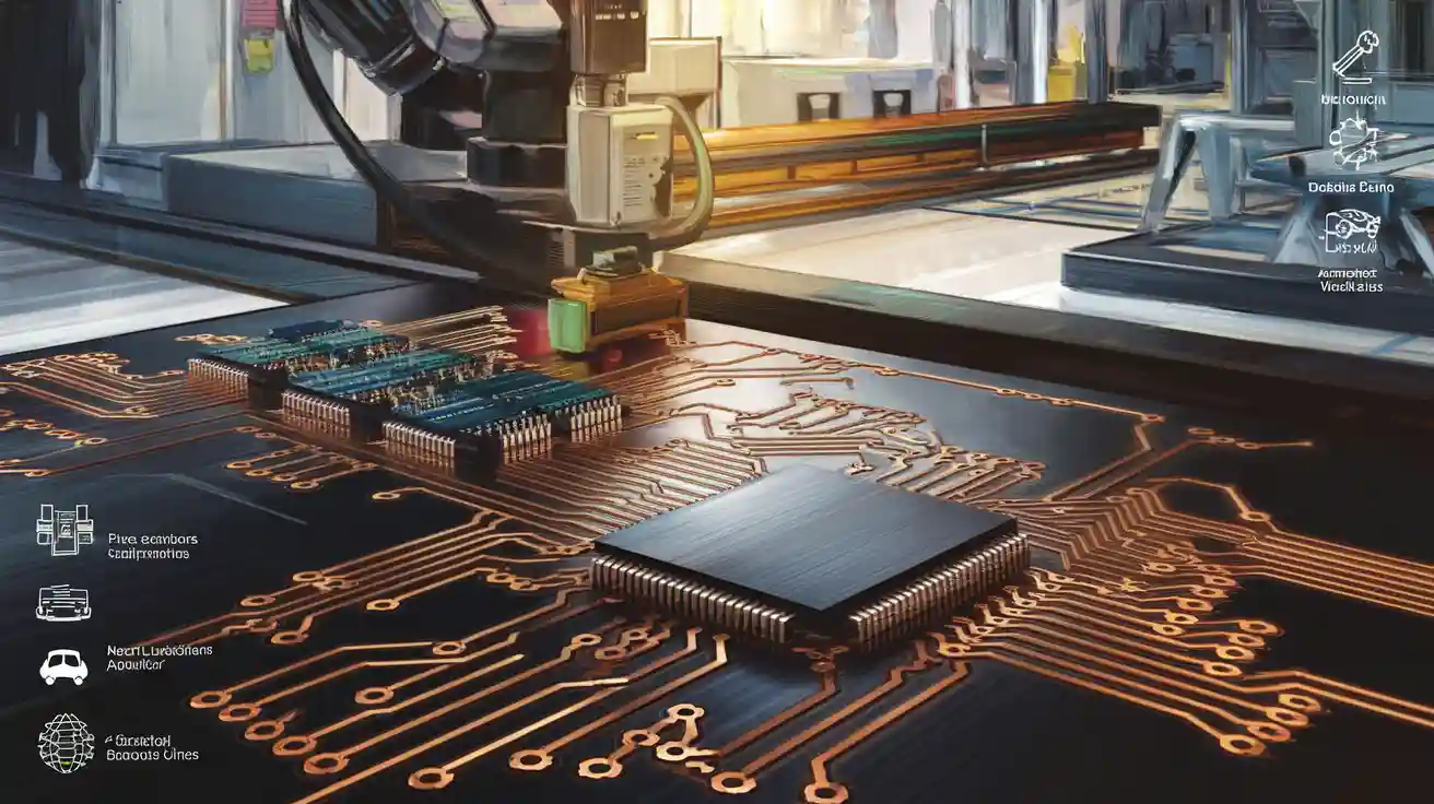
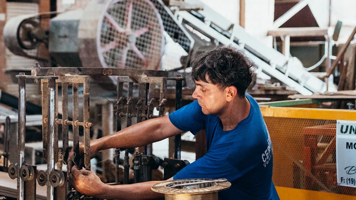
Manufacturing heavy copper PCBs presents significant manufacturing difficulties for engineers. Challenges arise when etching thick copper layers, and controlling plating and lamination processes is also tough. Selecting the right material is crucial, as metals like copper and brass are expensive and difficult to work with. Drilling through thick copper can result in rough holes or cracked pads, while lamination requires careful control to prevent weak bonding. Heavy copper PCBs are commonly used in power electronics, automotive, military, aerospace, and green energy applications due to their ability to handle high current and intense heat.
Key Takeaways
Heavy copper PCBs have thick copper layers. They can carry more current. They handle heat better. They last longer than standard PCBs.
Making heavy copper PCBs is hard. Etching, drilling, lamination, and coating need special care. These steps use advanced techniques.
Strict quality checks are important. People use visual inspection, X-rays, and electrical tests. These checks help find defects. They make sure heavy copper PCBs work well.
Heavy copper PCBs are used in many areas. They are in power electronics, cars, military, aerospace, renewable energy, and machines. They can handle high power and tough conditions.
Careful process control is needed. Using the right materials makes heavy copper PCBs stronger. This helps them last longer. It also lowers failures and maintenance costs.
What Is Heavy Copper PCB
Key Features
A heavy copper pcb is special because it has thick copper layers. Most people say a heavy copper pcb has copper that is 3 ounces per square foot or more. This is about 105 micrometers thick. You can see the usual copper weights and thickness in the table below:
Copper Weight (oz) | Copper Thickness (μm) |
|---|---|
3 oz or more | About 105 μm |
These boards can carry much more current than regular PCBs. They also get rid of heat better and are stronger. Heavy copper pcb designs are used where things need to be reliable and last a long time. Engineers pick them because they handle high power and do not get damaged by heat.
Note: Heavy copper pcb layers help stop overheating and lower voltage drops. This makes them great for hard jobs.
Standard vs. Heavy Copper PCB
The biggest difference between a standard PCB and a heavy copper pcb is the copper thickness and how they work. Standard PCBs have copper layers from 0.5 to 2 ounces per square foot. Heavy copper pcb layers start at 3 ounces and can be even thicker. The table below shows how they compare:
Property | Heavy Copper PCB | Standard PCB |
|---|---|---|
Copper Thickness | 3 oz/ft² and above | 0.5–2 oz/ft² |
Current-Carrying Capacity | Up to 200 A per channel | Below 10 A per channel |
Heat Dissipation | Superior | Limited |
Mechanical Robustness | High | Lower |
Manufacturing Process | Specialized techniques | Standard process |
Typical Applications | Power, automotive, industrial | Consumer electronics |
Heavy copper pcb technology lets more current flow and keeps things cooler. In one power plant, engineers saw that heavy copper pcb boards lasted three times longer than regular boards. This helped cut maintenance costs by 40% in five years. These facts show why many industries use heavy copper pcb for tough work.
Manufacturing Difficulties
Etching and Plating
Heavy copper pcbs need special etching and plating steps. Normal etching works for thin copper, but thick copper needs different ways. Makers use careful etching and do plating many times to get the right copper thickness. These steps make making the board harder and cost more money.
Thick copper makes it tough to control etching. There is a bigger chance of undercutting, which can mess up copper lines.
Chemicals move slower in thick copper, so engineers must change the process to stop mistakes.
One round of etching or plating is not enough for heavy copper pcb. Doing it many times helps the copper layer meet the right standards.
Designers use wider spaces and bigger lines to stop shorts and keep the board working well.
Tip: If copper is over 3 oz, makers should use special etching and plating to keep the board strong.
Lamination and Sealing
Lamination for heavy copper pcbs is hard. Thick copper and many layers need higher heat and longer time to cure. This helps the board stay stable, but it can also cause problems.
Some common lamination and sealing problems are:
Interfacial delamination: Layers come apart from bad lamination or wrong materials.
Intra-layer delamination: One layer splits, often from water or heat stress.
Surface delamination: The top blisters or lifts, caused by weak sticking or weather.
Internal delamination: Empty spots inside from bad resin or poor materials.
Microscopic delamination: Tiny empty spots from mistakes or rough handling.
The main causes are heat stress, water, bad materials, and dirt. Thick copper can bend during lamination, so spacing must be right. If layers do not expand the same way, it can pull pads off, crack lines, or bend the board. Engineers use gaps, matching materials, and heat tests to lower these risks.
Drilling Challenges
Drilling heavy copper pcbs is tricky. Thick copper wears out drill bits fast and makes cleaning out bits harder. Engineers change drilling settings, use drills for less time, and sometimes drill in steps to keep holes good.
Drill bits get dull fast with thick copper and rough foil.
Lubricants help lower friction and clear out chips.
Taking away or making inner pads bigger stops copper from pulling off.
CAM engineering changes hole sizes to keep them exact.
These steps help keep holes strong and lower mistakes.
Solder Mask and Coating
Putting solder mask and coatings on heavy copper pcbs is harder than on normal boards. Thick copper makes the surface bumpy, so it is tough to get an even coat. If the mask is not lined up right, copper pads can show or some spots may not be covered, which can cause shorts or rust.
Bumpy finishes like HASL make the mask thickness uneven.
Bubbles, cracks, and color changes can happen when putting on or drying the mask, making it weaker.
If the mask is too thin, copper is left open; if too thick, it can hurt how the board works and cools.
Heavy copper pcbs soak up heat during finishing, causing heat shocks. These shocks can make the mask peel or stick less.
Quality checks like stick tests, machine checks, and measuring thickness are needed to make sure the mask works well.
Quality and Inspection
Heavy copper pcbs need strict checks because they are complex. Makers use looking by eye, machine checks, X-rays, electric tests, heat pictures, and cutting boards to check inside.
Looking by eye and machine checks find surface mistakes, scratches, and missing parts.
X-rays show inside problems like empty spots, parts in the wrong place, and hole issues.
Electric tests look for shorts, open spots, and right resistance.
Heat pictures find hot spots that show solder or resistance problems.
Cutting boards shows inside details, but it destroys the board.
Common problems found are plating holes, not enough space at the edge, weak solder joints, copper bits, and open copper between pads. Careful checks and controls have made mistakes rare, but some still happen because heavy copper pcb making is hard.
Defect Type | Description | Prevention Strategies |
|---|---|---|
Plating Voids | Not enough metal in plated holes | Keep things clean, make hole walls smooth |
Insufficient Edge Clearances | Space too small near the edge | Use more space, check design |
Cold Solder & Joint Defects | Weak connections | Check process, use better materials |
Etching-Related Copper Slivers | Metal bits connect lines | Control patterns, wash well |
Exposed Inter-Pad Copper | Solder mask does not cover copper | Better mask, use more space |
Note: Using machine checks, X-rays, electric tests, and cutting boards together finds the most problems in heavy copper pcbs.
Solutions for Heavy Copper PCBs
Advanced Techniques
Manufacturers use special ways to fix problems with heavy copper pcb making. These ways help make the boards better and more reliable. Some of the best methods are:
Differential etching technology helps remove thick copper layers carefully. Engineers change etching steps to keep lines neat and steady.
Better drilling settings and tools make hole walls smoother. This also stops pads from cracking and keeps the board strong.
Careful control of heat and pressure during lamination helps resin flow right. This makes layers stick well and stops them from coming apart or bending.
Exact heat treatment takes away stress inside the board. This keeps the board’s material strong and helps it last longer.
Special soldering materials and ways make sure soldering works well, even with lots of copper.
Engineers use new machines for etching and lamination. They pick materials that can handle lots of heat and pressure. These smart ways let them make heavy copper pcb boards with copper over 10 oz/ft².
Process Control
Careful process control is very important in heavy copper pcb making. By watching each step, makers can get more good boards and make them last longer. Some key process control steps are:
Careful control of chemicals and heat during etching helps stop undercutting and keeps lines the same size.
Watching the etch factor helps the board stay the right size and work well.
Strong sticking between copper and the base stops layers from coming apart or bending.
Keeping a close watch on plating and etching times lowers mistakes.
Special machines and trained workers help keep quality high.
Controlling how the board grows with heat and how it handles soldering keeps it steady.
Tip: Good process control means fewer bad boards and heavy copper pcb products that last longer.
Applications of Heavy Copper PCBs

Power Electronics
Heavy copper pcb boards are very important in power electronics. Engineers use them in power supplies, electric cars, and solar inverters. Thick copper lets these boards carry more current and handle heat better. This helps devices work with lots of power without getting too hot.
Some main benefits in power electronics are:
Better at moving heat away from parts.
Can safely carry more current.
Stronger at connectors and holes.
Fewer failures when heating and cooling. For example, failure rates can drop from 32% to less than 1% after many cycles.
Heatsinks and big transformers can be put right on the board.
Boards can be smaller by using different copper thicknesses.
These things help make boards cooler and more reliable. That is why heavy copper pcb boards are used in power modules and fast computers.
Automotive
Car makers use heavy copper pcbs in electric cars, battery systems, and motor controls. These boards must last 10 to 12 years in tough places. They face heat, cold, water, and shaking. Makers test them with heating, cooling, and wet tests to make sure they are safe.
Main reasons for using heavy copper pcbs in cars:
They carry high currents, sometimes over 200 amps.
They get rid of heat well and stop overheating.
Strong design helps them survive shaking and bumps.
They meet strict quality rules like ISO 9001:2015.
The car industry uses many heavy copper pcbs. As electric cars and smart driving systems grow, more boards are needed. These boards work better and last longer than regular ones.
Military and Aerospace
Military and space systems need boards that never fail. Heavy copper pcbs are used in planes, satellites, flight tools, and defense radios. These boards must handle lots of power and survive shaking and harsh places.
Common uses are:
Power for military planes
Satellite and space gear
Flight and navigation tools
Drones and military robots
Defense radios and radar
Key needs are:
Carrying lots of current
Great at moving heat away
Strong against shock and shaking
Keeping signals clear and steady
Meeting military rules like MIL-STD-461
Heavy copper pcbs can use fewer layers for power, making designs simpler. They last a long time in hard jobs, so they are needed for important missions.
Renewable Energy
Solar and wind systems use heavy copper pcbs to handle high power. For example, a solar inverter may need to carry 50 amps or more. Boards with 6-8 oz copper can do this job.
Main jobs in renewable energy:
Carry lots of power all the time
Work well outside in changing weather
Help change and store energy
Stay strong and last many years
Heavy copper pcbs solve problems like heat, too much current, and stress. They help solar, wind, and battery systems work safely, even in bad weather.
Industrial Uses
Factories need boards that can carry lots of current and last through heat and shaking. Heavy copper pcbs are used in power converters, motor controls, trains, UPS, and welding machines.
Industrial Equipment Using Heavy Copper PCBs | Operational Advantages |
|---|---|
Power converters | Can carry more current |
Motor controllers | Better at moving heat |
Solar power converters | Stronger and tougher |
Rail traction systems | More reliable after many heat cycles |
UPS systems | Can mix high current and control circuits |
Excitation systems for power regulators | Handles big power and heat |
HVAC systems | Resists shaking and stress |
Fuse blocks | Stays stable in tough places |
High-power rectifiers | Lasts through heat and shaking |
Welding devices | Gets rid of heat and stays strong |
Heavy copper pcbs help machines resist heat and last longer. They do not need fixing as often. Their tough build helps them survive shaking, heat, and use, so machines last longer. This makes them a good pick for hard factory jobs.
Makers have a lot of problems when making a heavy copper pcb. They must do etching, drilling, and lamination very carefully. Changing the process helps the board last longer. It also stops heat from causing damage. Picking the right copper thickness is important. This helps the board work well and stay strong.
In tough jobs, these boards give steady power and can handle rough places.
When picking a maker, it is smart to check their certificates. You should also look at what other customers say. Make sure they use good machines and give strong help.
FAQ
What is the main reason to use heavy copper PCBs?
Engineers pick heavy copper PCBs because they carry lots of current. These boards also move heat away well. They work in tough places and last longer than regular PCBs. Heavy copper PCBs are more reliable for hard jobs.
How thick is the copper in a heavy copper PCB?
Heavy copper PCBs have copper that is 3 ounces per square foot or more. This is about 105 micrometers thick. Standard PCBs have much thinner copper layers.
What industries use heavy copper PCBs the most?
Heavy copper PCBs are used in power electronics, cars, military, planes, and green energy. These fields need strong boards for high power and heat.
Are heavy copper PCBs more expensive to manufacture?
Yes, heavy copper PCBs cost more to make. They use more copper and special ways to build them. Extra steps like etching, drilling, and lamination raise the price.
How do manufacturers check the quality of heavy copper PCBs?
Makers use many ways to check quality:
Looking at the board
Using machines to check for mistakes
X-ray checks
Testing with electricity
These checks help find problems and make sure the board is good.