

What Are RMS Noise, Standard Deviation, and SNR in Electronics and Why Do They Matter
RMS noise and standard deviation in electronics define signal clarity, impact PCB design, and help optimize SNR for reliable system performance.
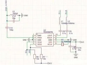
Radio Schematic Diagram Analysis Based on RDA5807M
This circuit Schematic Diagram is an FM radio receiver module built around the RDA5807M as the core IC. It mainly implements FM signal reception, audio output, and basic control functions. The analysis below is divided into core components, functional modules, and key design parameters. 1. Core Component and Pin Functions Core IC: RDA5807M The RDA5807M is a highly integrated FM radio receiver IC that supports FM broadcast reception and I2C / SDIO serial control. Based on the schematic, the key pins and their connections are summarized below: Pin Name Function Connected Component / Net Description ROUT Right-channel audio output Direct output (no extra components shown) Provides right-channel analog audio LOUT Left-channel audio output Direct output (no extra components shown) Provides left-channel analog audio RCLK Clock signal pin No explicit external connection (likely internal sync) Internal clock synchronization VDD Power supply input 3V3 power net 3.3V DC power supply GND Ground
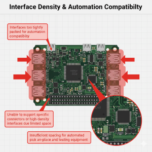
Industrial Tablet PC Case Study
Now, the demand for rugged mobile computing has surged as industries digitise their floor operations. Industrial tablets PC now serve as the backbone for smart warehouses and automated factories. These devices must operate where standard consumer electronics fail. Experts work hard to ensure these tablets withstand extreme vibration, dust, and moisture while maintaining a stable supply chain for long-term deployments. With an average lifecycle of five to seven years, industrial tablets require a hardware foundation that prioritises longevity over trendy aesthetics. Businesses hope these robust systems will reduce downtime and lower the total cost of ownership. Wonderful PCB provides the specialised engineering required to bridge the gap between complex board design and survival in the field. CUSTOMER CHALLENGES To begin, the client faced significant hurdles when developing their latest rugged tablet. Most off-the-shelf solutions lacked the specific interface density required for modern automation. First, of course, the device needed to

How to Troubleshoot and Optimize Your TV Signal Amplifier
Troubleshoot and optimize television signal amplifiers with easy steps to fix weak signals, reduce interference, and improve your TV reception fast.
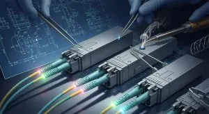
Fiber Optic Transceivers design and manufacturing
Fiber Optic Transceivers design and manufacturing covers key components, form factors, quality testing, and industry standards for reliable high-speed data transfer.

Cybersecurity Firewalls design and manufacturing
Cybersecurity Firewalls design and manufacturing ensure robust network protection, high performance, and compliance through advanced architecture and quality materials.
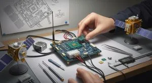
Satellite Navigation Equipment design and manufacturing
Satellite Navigation Equipment design and manufacturing ensures precise, reliable positioning through advanced engineering and strict quality standards.
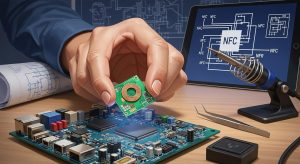
How to Design and Manufacture NFC Modules
Design and manufacture NFC Modules with optimal components, secure features, and robust testing for reliable performance in diverse applications.

Happy New Year from Wonderful PCB | 2026
As the New Year begins, all of us at Wonderful PCB would like to extend our sincere thanks to our customers, partners, and friends around the world. The past year has been a year of challenges, progress, and cooperation. With your trust and support, we continued to grow in PCB manufacturing, PCB assembly, flexible PCB, ceramic PCB, and electronic product design services. Every project, every inquiry, and every discussion has helped us move forward. In the coming year, we remain committed to: With over 30 years of industry experience, Wonderful PCB will keep focusing on long-term partnerships and practical solutions that help our customers succeed in their markets. We look forward to working closely with you in the New Year and creating more value together. Wishing you a successful, healthy, and prosperous New Year! Wonderful PCB Team

Best Practices for 5G Base Station PCB Manufacturing
5G Base Stations demand advanced PCB design, precise material selection, and strict quality control to ensure high-frequency signal integrity and reliability.
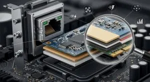
How the Choice of PCB Materials Impacts Network Adapter Performance
PCB material selection affects network adapter speed, signal integrity, and reliability, making it crucial for optimal performance in modern networks.

Design and Manufacturing of IP Phones
Design and manufacturing of IP phones ensures reliable business communication, integrating advanced hardware, software, and quality control for optimal performance.

The requirements of PCB design and manufacturing for optical communication equipment
PCB Design for optical communication equipment demands high-speed signal integrity, precise fabrication, and advanced material selection.

The design and manufacturing of modems
Modem design and manufacturing shape speed, efficiency, and reliability. See how modern design choices impact performance and the steps behind each modem.
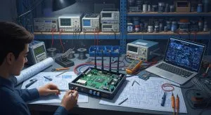
How to Design and Manufacture IoT Gateways for Industrial Use
Design and manufacture industrial IoT Gateways with robust hardware, secure connectivity, and scalable features for reliable factory performance.

5G PCB Design: High-Frequency Material Selection(Rogers, PTFE, LCP)
1. Introduction The success development of 5G PCB designs hinges critically on material selection. As 5G technology pushes frequencies into the millimeter-wave (mmWave) range of 24-77 GHz and beyond, traditional printed circuit board materials like standard FR-4 struggle to maintain signal integrity due to high dielectric loss and unreliable electrical properties. The selection of substrate material directly effects signal loss, thermal management, impedance control and reliability of 5G devices. Three primary material families dominate the 5G PCB landscape: Rogers high-frequency laminates, PTFE (polytetrafluoroethylene)-based substrates, and LCP (Liquid Crystal Polymer) materials. Each family offers distinct advantages in terms of electrical performance, mechanical properties, processing requirements, and cost. Rogers’s materials strike a balance between performance and manufacturability, PTFE-based laminates deliver the lowest losses for demanding applications, while LCP enables flexibility without compromising RF performance. 2. Key Material Properties for 5G Applications 2.1 Dielectric Constant (Dk/εr) The dielectric constant (Dk or εr) is

Step-by-Step Guide to Exporting Gerber Files From Any PCB Software
There are 8 standard steps to export Gerber files from any PCB software. These are: So this is basically a beginner guide that will share steps to export gerber files from any PCB software such as Kicad, Altium, Eagle, and Easy Eda. What Are Gerber Files? Gerber files are industry-standard files that contain layer-by-layer information about your PCB design. Each file describes a specific layer of your board. Your design software creates these files when you export your finished design. The files use ASCII text format that fabrication machines can read and process. Why Gerber Files Are Important for PCB Manufacturing Manufacturers rely on Gerber files to control every step of PCB fabrication. The files tell machines where to etch copper traces, drill holes, and apply solder mask. Without proper Gerber files, your manufacturer cannot build your board. How often do you check your files before sending them to production?
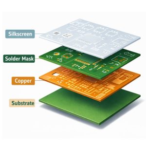
Common Gerber Layers Explained
Gerber layers are individual vector graphic files. These files tell how your Printed Circuit Board will look. Gerber files tell physical aspects like copper traces, solder masks, and silkscreen. PCB manufacturers use these files to control every production step. You view these layers stacked from top to bottom, with the bottom layers mirrored for accurate fabrication. Individual Files for Each Layer Every real part of your PCB needs its own Gerber file. Like, you must have separate files for the top copper, the bottom copper, the paint for solder masks, the white silkscreen words, and the paste layers. If your PCB is a multilayer, you also need files for the inner copper layers! Every single layer is a separate file. This helps the factory to work on each part alone. Viewing Gerber Layers When you look at these files using a special online viewer, the software shows them all stacked
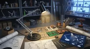
Smart Desk Lamps design and manufacturing
Smart Desk Lamps combine advanced design, energy-saving LEDs, and smart features for efficient, user-friendly lighting and sustainable manufacturing.

The design and manufacturing of AI phones
AI Phones feature advanced hardware and on-device AI, enabling smart functions, efficient manufacturing, and improved user privacy.