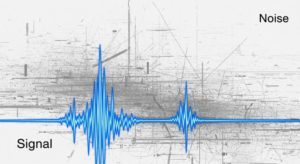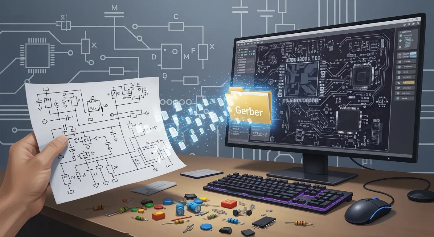
When you want to make your electronic idea real, you need to change the schematic into a Gerber file. A schematic shows how the parts connect. A Gerber file tells machines how to build the board. Look at the table below to see the main differences:
Aspect | Schematic Files | Gerber Files |
|---|---|---|
Purpose | Electrical connections and logic | Physical layout and fabrication instructions |
Information Conveyed | Relationships among parts | Layer details, outlines, and drill data |
File Composition | One file for the circuit | Several files for each board layer |
You use PCB design software to go from schematic to Gerber. To do this, you follow these steps:
Make a job file in your project.
Pick which manufacturing files you need.
Choose the right layers to export.
Check the Gerber files for mistakes.
Tip: Clear file names and correct formats help stop problems during manufacturing.
Key Takeaways
Know that schematic files and Gerber files are not the same. Schematic files show how things connect. Gerber files tell machines how to make the board.
Use PCB design software to change your schematic into Gerber files. Follow each step so you include all layers and details.
Always look at your Gerber files with a viewer before sending them out. This helps you find mistakes and stops expensive problems.
Talk clearly with your PCB manufacturer. Give them all the files and details they need for smooth work.
Run Design Rule Checks (DRC) in your software to spot and fix problems early. This step saves time and makes your final product better.
Schematic to Gerber Overview
What Is a Schematic?
You begin your printed circuit board design with a schematic. This is a picture that shows how parts connect and work together. In PCB design, a schematic is a drawing that shows how the circuit board works. You see symbols for things like resistors, capacitors, chips, and wires. These symbols help you see how electricity moves and how your project works. When you look at a schematic, you can find mistakes or missing connections before you move on.
What Are Gerber Files?
After you finish your schematic, you need to make gerber files. These files tell machines how to build your board. Each gerber file gives instructions for a different part of the board. You will have files for copper layers, solder masks, silkscreens, and holes. Here is what you usually include:
Top layer image of copper conductor on the PCB
Bottom layer image of copper tracks on the PCB
Image of the solder mask for the top layer
Image of the bottom layer solder mask
Image for the silkscreen on top layer
Image for the silkscreen on bottom layer
Information about holes, like where they are and what they do
Internal cut-outs and other machining steps
A file that tells the name and purpose of each file above
You need all these files to make sure your board is made the right way.
Why Gerber Files Matter
Gerber files are very important in the schematic to gerber process. Manufacturers use these files to build your board correctly. You get fewer mistakes and better boards. Gerber files give detailed design information that helps manufacturers make good circuit boards. They work with many CAM tools, so you can send your files to different companies easily. The standard format helps stop confusion and saves time. Gerber files are used all over the world, so everyone can work together. You make things go faster and smoother when you use the right files.
Tip: Always check your gerber files before sending them to be made. This step helps you avoid expensive mistakes and delays.
Getting Your Schematic Ready
Schematic Capture (Making or Importing a Schematic)
You begin your PCB design by doing schematic capture. This means you make or bring in a drawing that shows how all the parts connect. Schematic capture lets you plan your project before you build the real board.
Popular Software Choices: KiCad, EasyEDA, Altium Designer, Eagle, OrCAD
There are many PCB design tools for schematic capture. Here are some popular ones:
KiCad: Free and open-source. It has good features for new and skilled users.
EasyEDA: Works online and is simple to use. It is good for beginners and lets you work with others online.
Altium Designer: Has advanced tools and is easy to use. Many professionals use it.
Eagle: Makers and small teams like it. It works with Autodesk and supports cloud projects.
OrCAD: Used in industry and is powerful. It has strong tools for testing and checking circuits.
DipTrace: Simple to use and lets you see 3D models. It is good for both new and advanced users.
Tip: Try out different software to find what fits your skills and needs.
When you make a schematic, you do these steps:
Gather Requirements: Decide what your circuit should do and how much power it needs.
Select Components: Choose parts that fit your project. Look at datasheets for more info.
Create Component Symbols: Use the software’s library or make your own symbols for each part.
Connect Components: Draw wires to join the parts. Check that every connection is right.
Design Rule Check (DRC): Run a check to find missing or wrong connections.
Error Checking and Netlist Generation
You need to check your schematic for mistakes before moving on. Most PCB design software has tools for this. Design rule checks (DRC) help you spot problems like missing wires or wrong pins. Fixing these early saves you time and money.
After you check for mistakes, you make a netlist. A netlist is a list that shows how every part connects in your circuit. It has net labels, reference names, and pin numbers. The netlist links your schematic to the PCB layout. You need a correct netlist to go from schematic to gerber files without errors.
Note: Always look over your netlist before starting the PCB layout. This step helps you avoid big mistakes later.
Common Schematic Mistakes
Many people make the same mistakes when making schematics. Watch out for these problems:
Missing or wrong connections between parts
Using the wrong symbols for parts
Forgetting to label nets or signals
Wires that cross and cause confusion
Not running the design rule check
You can avoid these mistakes by checking your work and using the error-checking tools in your software.
Software | Best For | Key Features |
|---|---|---|
KiCad | All users | Free, open-source, feature-rich |
EasyEDA | Beginners | Web-based, easy, cloud collaboration |
Altium Designer | Professionals | Advanced, industry standard |
Eagle | Makers, small projects | Autodesk integration, user-friendly |
OrCAD | Industry, simulation | Powerful, strong analysis tools |
DipTrace | Beginners, professionals | 3D modeling, easy to use |
You can do well in the schematic to gerber process by picking the right software, checking for mistakes, and avoiding common errors.
PCB Layout from Schematic
Schematic to PCB Layout
You use design software to go from schematic to PCB layout. The software lets you pick and move parts in a schematic editor. You can use old designs again and link parts of your schematic. This helps you with big projects. When your schematic is done, you put it on a blank PCB layout. The software brings in part data and design rules. This lets you start building your printed circuit board fast. This step is important in the schematic to gerber process.
Tip: Try using KiCad, Altium Designer, or EasyEDA to keep your work neat and easy.
Component Placement and Routing
You must put each part on the PCB in a smart way. Good placement makes your board work well and helps with making it. Put parts that go together close to each other. Connect signal traces to match the nets in your schematic. Use short and straight traces when you can. For hard boards, use horizontal and vertical traces on different layers.
Here are some good tips for routing:
Route high-speed signals over a solid ground plane.
Put vias in a grid to stop hot spots.
Use 135-degree bends for traces to stop heat traps.
Make space between traces bigger to stop shorts.
Keep analog and digital ground planes apart to lower noise.
Make high-current paths wider to stop heating.
Connect decoupling capacitors right to IC pins.
Note: Placing and routing parts with care helps you avoid problems when making gerber files.
Design Rule Checks
Before you export your gerber files, run a Design Rule Check in your PCB software. DRC finds problems like spacing mistakes and small trace widths. Always use a standard layer naming system and check layer names again. These checks help you find mistakes early and make sure your PCB is ready for manufacturing.
Design Rule Check | Why It Matters |
|---|---|
Spacing | Stops shorts and crosstalk |
Trace Width | Stops broken connections |
Layer Naming | Makes file export correct |
Tip: Run DRC before exporting gerber files to save time and money.
Export and Verify Gerber Files
Export Gerber Files
You need to export your design into gerber files before you send your printed circuit board for manufacturing. This step is important because manufacturers use these files to build your pcb. Each pcb design software has its own way to export files, but the process follows a similar pattern. Here is how you can do it in some popular tools:
Open your pcb layout in the software.
Go to the menu and find the option to export or plot files.
Choose the output directory where you want to save your files.
Select all the layers you need for manufacturing.
Set the options for standard gerber file formats.
Adjust extra settings for better results.
Click the button to generate the files.
Create drill files for holes and vias.
Check the file path to make sure the files are there.
You must follow these steps in tools like KiCad, Eagle, and Allegro PCB Editor. For example, in Eagle, you open the .brd file, use the Cam Processor, select the right job file, and make sure you add gerber file for each layer. In KiCad, you use the Plot menu, pick the layers, and create drill files. In Allegro, you use the Artwork tool, add all needed layers, and set the parameters before you create the artwork.
Tip: Always double-check your output directory and file names. This helps you avoid confusion and missing files.
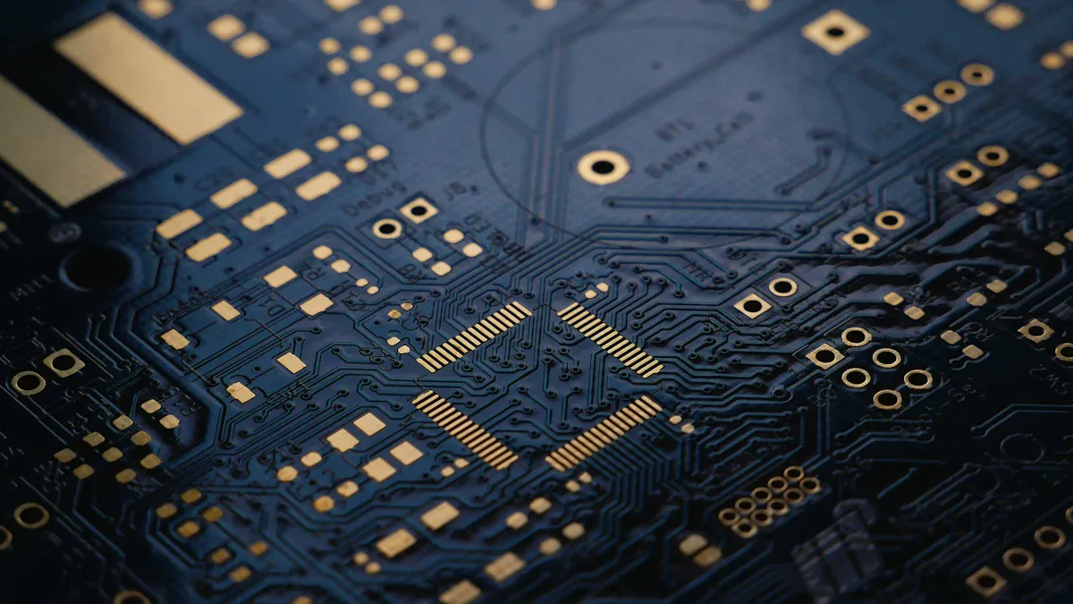
Include All Layers and Outlines
You must include every layer and outline in your gerber files. Missing a layer can cause your pcb to fail or not work as you want. Here is a list of layers you should include:
Top copper layer (TOP)
Bottom copper layer (BOT)
Solder mask top (SMT)
Solder mask bottom (SMB)
Solder paste top (SPT)
Solder paste bottom (SPB)
Silkscreen top (SST)
Silkscreen bottom (SSB)
Assembly top (AST)
Assembly bottom (ASB)
Fabrication layer (FAB) for details like drills, cutouts, and stack-up
Aperture definitions
Board outline
You need to make sure you use the right format for each file. The format for each layer must match what your manufacturer expects. If you use the wrong format, the machines may not read your files. Always check the format for drill files and outlines. Some manufacturers want Excellon format for drill files and RS-274X format for layers.
Note: If you forget to include a board outline or drill file, your pcb may not be made correctly.
Verify with Gerber Viewer
After you export your gerber files, you must check them with a gerber viewer. This tool lets you see your files as the manufacturer will see them. You can find free gerber viewers online. Open each file and look for problems. Here are common errors you might find:
Design mismatch between layers
Insufficient clearances between traces or pads
Obsolete or wrong file formats
Unregistered or misaligned layers
Incomplete files or missing layers
Incorrect aperture lists
Layer mislabeling
Missing drill files or board outline
Solder mask misalignment
Zero-width traces
Empty or corrupted data
Ambiguous file names
You need to fix these errors before you send your files to the manufacturer. If you see missing holes, wrong outlines, or strange colors, go back to your pcb design and export the files again. Always use the correct gerber file formats for each layer. This step in the schematic to gerber process helps you avoid delays and extra costs.
Tip: Use a gerber viewer every time you finish exporting. This simple check can save you from big mistakes.
Submit Gerber Files for Manufacturing
Prepare Files for Submission
You need to get your files ready before sending them to a pcb manufacturer. First, check all your files to make sure nothing is missing. Put your Gerber files, drill files, and other documents in one ZIP folder. This keeps your project neat and easy to look at. Most manufacturers want files in formats like RS-274X for Gerber and Excellon for drill data. You should add a Readme file if you have special notes or instructions.
Here is a table that shows the files you should include:
File names | Description |
|---|---|
Stack-up | Shows the order of layers on the board |
Excellon drill file | Has tool codes and X-Y spots for all holes |
Drill tool list | Lists the tools needed for drilling |
Top, bottom, internal copper | Shows the metal traces on the pcb |
Solder mask (top/bottom) | Has data for the solder mask layers |
Silkscreen (top/bottom) | Shows part names and markings |
Board outline & milling | Shows the size, cutouts, and shape of the board |
Aperture/D-Code list | Needed if you do not use RS-274X format |
Solder paste areas | Shows where to put solder paste |
DXF/DWG files | Extra CAD files for reference |
Special instructions | Any extra rules for the pcb manufacturer |
Tip: Open your files in a Gerber viewer before you zip them. This helps you find missing or wrong layers.
Communicate with Manufacturer
You must give your pcb manufacturer all the right information. Good communication helps stop mistakes and makes things faster. When you send your files, include:
All design files, like Gerber and drill files
A Readme file with board details and special needs
Info about the board stack-up and materials
Notes about surface finish, solder mask color, and silkscreen color
Any special rules, like “Do not mirror layers”
Ask your manufacturer if they can do a DFM check. This check finds problems before they start making your board. If you have questions, talk to your manufacturer early. They can help you fix problems and make sure your pcb is made right.
Final Tips for Success
Follow these steps to make your pcb order go well:
Add all needed files, like Top Silkscreen, Top Copper, Bottom Copper, NC Drill, and Board Outline.
Put in a Readme file to explain your design and special requests.
Run a DFM check to make sure your design fits the manufacturer’s rules.
Use a Gerber viewer to check that all files open and look correct.
Make sure your traces and spaces are big enough for your pcb manufacturer.
Use clear file names and the right formats.
Stay in touch with your manufacturer to fix problems quickly.
Many pcb manufacturers have free tools and guides to help you. Use these to check for shorts, missing layers, or wrong spaces. Careful checks and good communication help you get a great printed circuit board every time.
You can do well in PCB design if you follow each step. Always look at your files with a Gerber viewer. Make sure your trace widths are correct. Include every layer in your files. The table below shows how checking your work helps you:
Benefit | Impact |
|---|---|
Success Rate Increase | Over 95% first-pass success |
Cost Implications | Avoids costly mistakes |
File Confirmation | Ensures design rule compliance |
Try using special design rules to make your board better. You should also talk to manufacturers to get help and stop mistakes.
FAQ
What is the difference between a schematic and a Gerber file?
A schematic shows how parts connect in your circuit. A Gerber file gives instructions to machines for making your printed circuit board. You use the schematic to design, and you use the Gerber file to manufacture.
Can I use free software to create Gerber files?
Yes, you can use free tools like KiCad or EasyEDA. These programs let you design your circuit and export Gerber files for manufacturing. Many hobbyists and students use them for their projects.
What should I check before sending Gerber files to a manufacturer?
You should open your Gerber files in a viewer. Check for missing layers, wrong outlines, or errors. Make sure you include drill files and a board outline. Clear file names help avoid confusion.
Why do manufacturers need drill files along with Gerber files?
Drill files tell machines where to make holes for parts and vias. Without these files, your board will not have the right holes. Always include them with your Gerber files.