Project Overview
The Personal Digital Assistant (PDA) project showcases Wonderful PCB’s comprehensive capability in developing professional-grade handheld devices. This case study describes the complete development of an industrial smart terminal designed for data collection, communication, and operational task management in professional environments including warehousing, retail, field service, and healthcare.
Wonderful PCB provided end-to-end turnkey services covering electronic hardware design, multi-layer PCB layout and manufacturing, PCBA assembly with SMT and BGA components, and comprehensive testing protocols. This integrated approach enabled the customer to streamline development, reduce coordination overhead, and accelerate time-to-market while maintaining strict quality standards.
Project deliverables included: complete hardware architecture design and component selection, 8-layer HDI PCB design and manufacturing, SMT/BGA assembly with >98% first-pass yield, functional and reliability testing, and design optimization for volume production.
Customer Requirements and Challenges
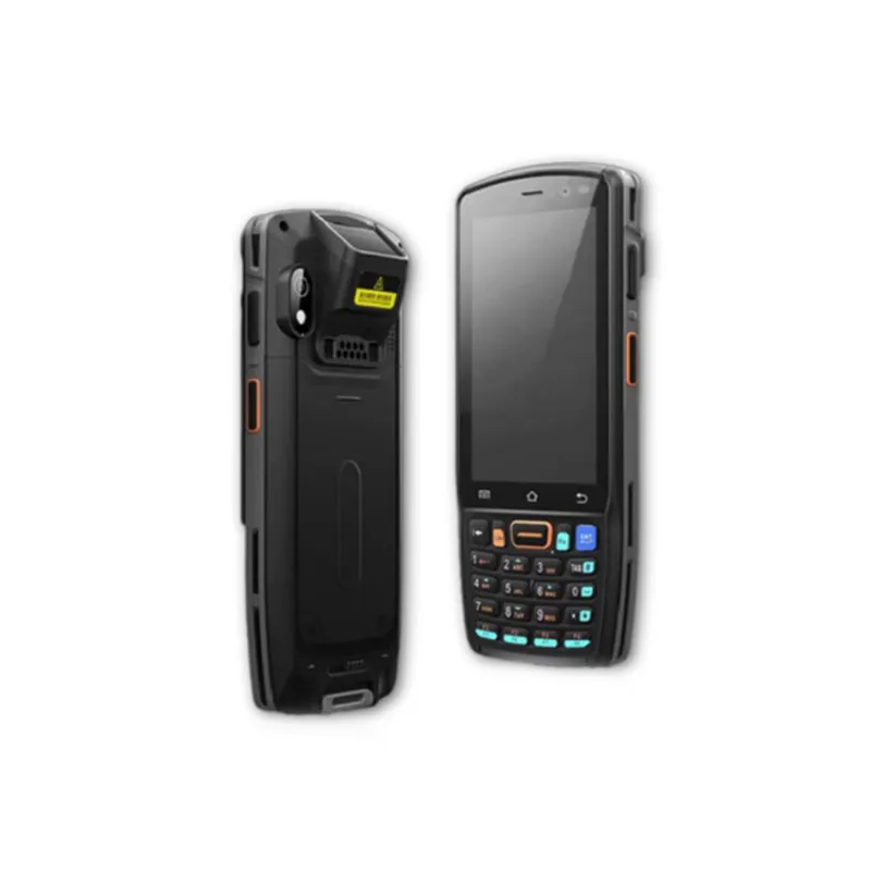
A sample scenario is described here. The customer required a ruggedized handheld terminal capable of reliable operation in demanding industrial environments. Key specifications included: ARM Cortex-A processor with 2GB RAM and 16GB storage, 5-inch sunlight-readable touchscreen (450+ nits), integrated 1D/2D barcode scanner, dual-band Wi-Fi and Bluetooth 5.0, optional 4G LTE connectivity, 4000mAh battery providing 10+ hours operation, IP65 dust and water resistance, and 1.5-meter drop resistance.
Main Technical Challenges:
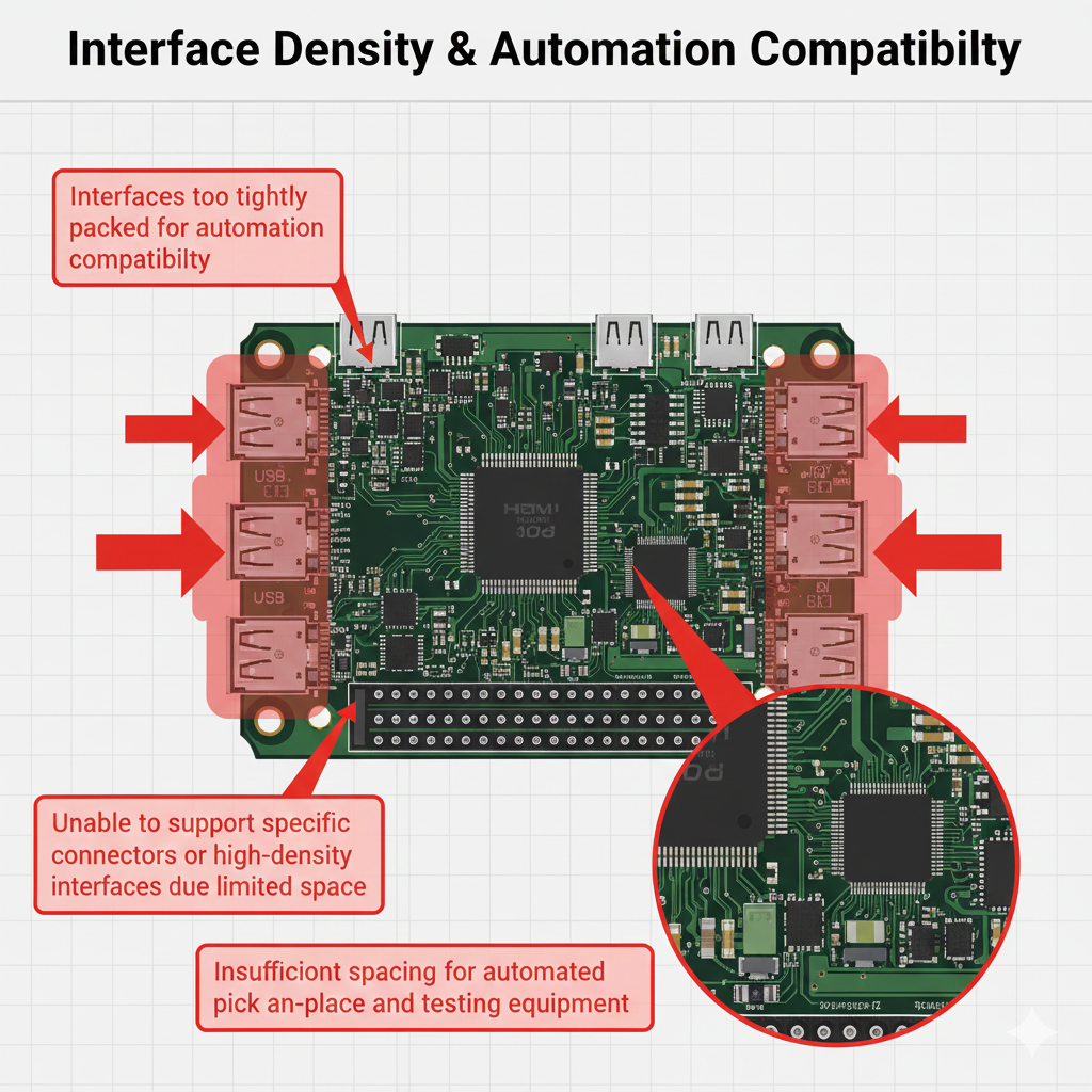
The project presented significant engineering challenges. The compact form factor (150mm × 75mm × 20mm) required extreme component density with over 500 components on the main PCB while maintaining signal integrity and thermal management. Simultaneous operations of Wi-Fi, Bluetooth, and LTE in close proximity demanded careful RF design to prevent interference and ensure FCC/CE compliance. Achieving 10+ hours battery life requires sophisticated power management with multiple voltage domains and dynamic power scaling. High component density with large BGA packages and fine-pitch components (0.4mm pitch) necessitated careful design-for-manufacturing optimization to support automated assembly with high yields.
Wonderful PCB’s Solution
1 Hardware Architecture Design
The hardware architecture centered on a high-performance ARM Cortex-A quad-core processor optimized for mobile applications. The design integrated 2GB LPDDR4 RAM for responsive performance, 16GB eMMC storage with microSD expansion capability, multi-channel PMIC providing efficient power regulation, certified Wi-Fi/Bluetooth combo module reducing RF design risk, and optional LTE modem with global band coverage. Peripheral interfaces included USB Type-C with Power Delivery support, dedicated UART for barcode scanner integration, and comprehensive ESD protection on all external connections.
2 PCB Design and Layout
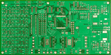
The 8-layer PCB stackup provided optimal signal integrity and power distribution. Layer 1 (Top) handled high-density component placement and routing. Layers 2 and 7 served as solid ground planes for signal returns and EMI shielding. Layers 3 and 6 routed high-speed differential pairs and critical signals. Layers 4 and 5 distributed power with low impedance. Layer 8 (Bottom) accommodated additional components and routing.
Critical design features included length-matched DDR4 traces maintaining ±25 mils tolerance for reliable memory operation, 50Ω controlled impedance for USB and RF signals, strategic RF module placement at board edges with dedicated ground vias and keep-out zones, comprehensive power distribution network with strategic decoupling capacitor placement, and thermal vias connecting the processor thermal pad to internal ground planes for heat dissipation.

3 PCB Manufacturing
Wonderful PCB’s in-house manufacturing facility produced the 8-layer boards with 5mil/5mil trace/space capability, 1oz copper weight (2oz on power layers), ENIG surface finish for excellent solderability, and controlled impedance tolerance within ±10%. Quality control included automated optical inspection (AOI) detecting trace defects, flying probe electrical testing verifying continuity and isolation, time-domain reflectometry (TDR) validating controlled impedance, and microsection analysis confirming internal layer quality and registration.
PCBA Assembly and Component Sourcing
PCBA assembly utilized advanced SMT equipment placing 50,000+ components per hour with fine-pitch capability down to 0.3mm pitch. The process included high-precision solder paste printing with SPI verification, automated pick-and-place with submicron accuracy for BGA components, lead-free reflow soldering in nitrogen atmosphere, and X-ray inspection verifying BGA solder joint quality. Multi-stage quality control achieved >98% first pass yield after process optimization.
Component sourcing leveraged relationships with authorized distributors (Arrow, Avnet, Digi-Key) ensuring authentic parts with full traceability. Critical ICs sourced exclusively from authorized channels eliminated counterfeit risk. Second-source options specified for passive components provided supply chain flexibility. Incoming quality control verified component authenticity before acceptance into inventory.

Testing and Quality Control
Comprehensive testing validated product reliability. Functional testing verified system boot, touchscreen calibration, barcode scanner performance across all standard symbologies, button/LED functionality, and USB data transfer and charging. Wireless communication testing measured Wi-Fi/Bluetooth RF performance in shielded chambers, validating output power, receiver sensitivity, and data throughput against IEEE 802.11 specifications. LTE cellular testing (optional models) confirmed band coverage and carrier compatibility.
Power and battery testing measured charge current profiles, runtime validation (achieving 12 hours vs. 10-hour target), and battery protection circuitry verification. Environmental and reliability testing included temperature cycling (-10°C to +50°C), drop testing (1.5 meters, 26 drops per IEC 60068-2-32), vibration testing per IEC 60068-2-64, IP65 validation through dust chamber and water spray testing, and accelerated aging at elevated temperatures.
Quality metrics demonstrated manufacturing maturity: First Pass Yield >98%, DOA Rate <0.5%, Field Failure Rate <1% within 90 days, and zero critical defects in pilot production shipments.
Final Product Features
The final PDA delivered professional-grade specifications: ARM Cortex-A quad-core @ 1.5GHz with 2GB LPDDR4 RAM and 16GB eMMC storage (expandable to 128GB), 5.0-inch capacitive touchscreen (1280×720, 450 nits, 10-point multi-touch), integrated 1D/2D barcode scanner (5cm to 50cm range), dual-band Wi-Fi 802.11ac and Bluetooth 5.0 with optional 4G LTE, USB Type-C with Power Delivery charging, 4000mAh battery providing 10-12 hours runtime, IP65 dust and water resistance, -10°C to +50°C operating temperature, and 1.5-meter drop resistance.
Key product advantages included responsive performance from optimized hardware/software integration, industry-leading battery life through sophisticated power management, robust RF connectivity maintaining strong signals in challenging environments, ruggedized construction withstanding daily abuse in industrial settings, and ergonomic design enabling comfortable one-handed operation during extended shifts.
Project Results and Benefits
The integrated development approach delivered significant customer value. Development efficiency improved through single-point accountability, eliminating multi-vendor coordination overhead and reducing overall timeline by 25-30% compared to previous projects. Cost optimization achieved 15-20% savings through consolidated sourcing, in-house manufacturing avoiding external margins, and high first-pass yield minimizing rework costs.
Quality and consistency remained high throughout prototype and production phases. Prototype units accurately represented production performance, preventing the common scenario where prototypes work but production units fail. Technical success metrics included: 7 months from concept to pilot production, only 2 hardware revisions required, >98% production yield, <0.5% DOA rate, <1% field failure rate within 90 days, 12-hour battery life exceeding targets, and successful FCC/CE certification on first submission.
Why Wonderful PCB
Wonderful PCB offers comprehensive advantages for electronic product development. Our one-stop solution eliminates vendor coordination complexity, providing electronic design, PCB manufacturing, PCBA assembly, component sourcing, testing, and engineering support under one roof. In-house manufacturing facilities ensure direct quality control, rapid prototyping capability, and flexible scheduling. Experienced engineering teams bring expertise across high-speed digital design, RF circuits, power management, thermal design, and EMC/EMI compliance. Strong component sourcing relationships with major distributors secure authentic parts at competitive pricing. Flexible production support scales from prototype quantities (5-10 units) through volume production (thousands monthly), allowing customers to start small and scale gradually without changing suppliers.
Application Scenarios
The PDA platform focuses on diverse market needs. Logistics and warehousing utilize the device for inventory tracking, receiving/shipping verification, and order picking with real-time wireless updates. Retail stores employ it for price verification, inventory checks, and mobile checkout. Field service technicians access documentation, record activities, and identify parts with ruggedized reliability. Healthcare facilities use it for patient identification, medication verification, and specimen tracking with antimicrobial-compatible materials. Manufacturing applies it to work order tracking, quality control data collection, and assembly verification. Transportation companies utilize it for package scanning, proof-of-delivery, and GPS-enabled route optimization. Flexible architecture supports customization while maintaining common core electronics reducing variant development costs.
Conclusion
This PDA case study demonstrates Wonderful PCB’s comprehensive capability delivering sophisticated handheld electronic devices from concept through volume production. Such factors successfully overcame significant technical challenges including space-constrained high-density design, RF coexistence in compact housings, extended battery life requirements, and manufacturing at volume with high yields. Key factors included close engineering collaboration, comprehensive design-for-manufacturing approach, in-house quality control, rigorous testing protocols, and flexible production support. The resulting product met all requirements while exceeding performance targets, establishing Wonderful PCB as a trusted long-term manufacturing partner.
If you are developing a handheld device, portable instrument, or mobile computing platform, Wonderful PCB stands ready to support your project with comprehensive design and manufacturing services. Contact us to discuss your requirements, receive expert recommendations, and get quotations for design services, prototypes, or production volumes.