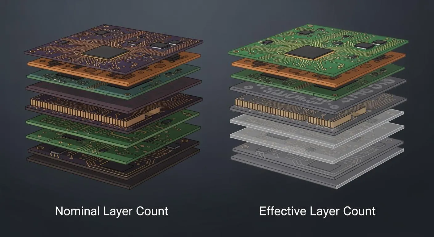
You might see the term layer count in pcb design and wonder what it really means. Nominal layer count shows how many copper layers the manufacturer will build into your board. Effective PCB Layer Count tells you how many layers actually carry signals, power, or ground in your design. Not every layer will help your circuit work. If you know the difference, you can avoid mistakes in your design and make sure your board works as planned.
Key Takeaways
Learn the difference between nominal and effective PCB layer counts. Nominal means all layers. Effective only counts layers with signals, power, or ground.
Always look at your stack-up drawing before making the board. This helps your design match the nominal layer count. It also stops confusion.
Find effective layers by checking what each layer does. Only count layers that help with signal flow, power, or grounding.
Talk clearly with your fabricator about your design. Tell them what each layer does. This helps stop mistakes when making the board.
Think about layer count when you plan your PCB design. Balancing cost, performance, and making needs helps your board work better and last longer.
Nominal PCB Layer Count

Definition and Specification
You will see the term nominal layer count in many PCB design documents. This number tells you how many copper layers your board will have from the manufacturer. For example, if you order a 4-layer PCB, the nominal layer count is four. Each layer sits on top of or below another layer inside the board. Manufacturers use this number to plan the stack-up and build the board.
You can find the nominal layer count in the stack-up drawing. This drawing shows the order of each layer, including signal, power, and ground layers. You should always check this drawing before you send your design for manufacturing. If you work with multilayer boards, you will see higher numbers like 6, 8, or even 12. These numbers help you and the manufacturer talk about the same thing.
Tip: Always match your design files to the nominal layer count in your stack-up drawing. This step helps you avoid confusion later.
Common Misconceptions
Many people think the nominal layer count means every layer does something important. This idea is not always true. Some layers might not carry signals or power. You might see a layer that only acts as a shield or a dummy layer. These layers still count in the nominal number, but they do not help your circuit work.
Here are some common mistakes you should avoid:
Believing every layer in the count is used for signals or power.
Ignoring unused or dummy layers in your design.
Assuming all manufacturers use the same rules for counting layers.
You should always check what each layer does in your design. Do not trust the nominal layer count alone. Look at the stack-up and see which layers are effective. This habit will help you make better choices in your pcb design and avoid problems with your multilayer boards.
Effective PCB Layer Count
What Makes a Layer Effective
It is important to know what makes a layer effective. The effective pcb layer count shows how many layers help your circuit work. These layers carry signal, power, or ground. Do not count layers that do not have a real job in your design. The effective pcb layer count depends on a few things:
Circuit complexity: Harder circuits need more layers for all the signals.
Space constraints: Small boards mean you must use each layer well.
Power requirements: High-power designs need more layers for power and heat.
Future expansion: You might add layers for upgrades or changes later.
When you think about the effective pcb layer count, your design gets better. Every layer should help with signal flow, power, or grounding.
Signal, Power, and Ground Layers
You need to know how each layer helps the effective pcb layer count. Each type of layer has its own job. The table below shows the main types and what they do:
Layer Type | Purpose |
|---|---|
Signal Layer | Carries signal traces between components. |
Ground Plane | Reduces electromagnetic interference and keeps signal integrity strong. |
Power Plane | Delivers power across the board and supports integrity. |
Internal Layers | Adds routing options for dense designs and helps with integrity. |
Bottom Layer | Completes signal paths and connects parts. |
Put signal layers next to ground planes to keep signals safe. Pick materials that keep electrical and thermal integrity high. Always balance copper layers to stop the board from warping.
Dummy and Unused Layers
Dummy or unused layers do not count in the effective pcb layer count. You might see these layers in multilayer boards to fill space or balance copper. They help keep the board flat and stop thermal stress. Sometimes, you add a dummy layer to make an odd layer count even. This step can lower costs and help with manufacturing. Dummy layers do not carry signal, power, or ground, so they do not help with signal integrity or your circuit’s integrity.
Pseudo or Fake Layer Count Issues
What Is a Pseudo 6-Layer PCB
Sometimes, people use the word “pseudo” when talking about PCB layers. A pseudo 6-layer PCB looks like it has six layers. But it is not built the same way as a real 6-layer board. Manufacturers use this trick to fix problems like crosstalk in normal boards. For example, a pseudo 8-layer stackup uses three cores. The middle core gets removed, so there is more space between layers. This extra space helps stop crosstalk and makes coupling better. Even if the board only has six copper layers, people still call it a “pseudo 8-layer board.” This is because it is made almost the same way as a real 8-layer board. The price is about the same as a true 8-layer board since the steps are similar.
You might pick a pseudo layer count for special design needs. But you should know that the number of layers is not always the same as the number of working copper layers. Always look at the stack-up drawing to see which layers carry signals, power, or ground.
Real-World Risks and Pitfalls
Using a pseudo 6-layer PCB can cause problems, especially in designs that must be very reliable. You might have trouble with how your board works. The table below shows some common risks and what could go wrong:
Risk Type | Specific Issues |
|---|---|
Signal integrity issues | Severe ringing in important signals |
Eye diagram tests do not pass | |
System bit error rate goes over the limit | |
Power stability problems | Voltage changes go past safe levels |
You hear a lot of switching noise | |
EMC test failures | Too much radiation leaves the board |
Immunity tests do not work out | |
Thermal management difficulties | Some spots get too hot and cannot cool down |
You need more thermal layers or vias |
You should always talk to your manufacturer before picking a pseudo layer count. If you do not check the real board structure, your board might fail signal tests or get too hot. Checking each layer carefully helps you avoid these problems and make a board you can trust.
Comparing Nominal and Effective Layer Count
Key Differences
You need to know the main differences between nominal and effective layer count. These differences help you avoid mistakes in pcb design. The table below shows how each type of layer count works:
Feature | Nominal Layer Count | Effective Layer Count |
|---|---|---|
What it means | Total number of copper layers built | Number of layers that carry signal, power, or ground |
Where you find it | Stack-up drawings and fab notes | Actual design files and routing |
Used for | Manufacturing and quoting | Electrical performance and layout |
Includes dummy layers? | Yes | No |
Affects signal flow? | Not always | Yes |
You see that nominal layer count tells you how many layers the manufacturer will build. Effective layer count tells you how many layers help your circuit work. Dummy or unused layers count in the nominal number, but not in the effective number. Only layers that carry signal, power, or ground count as effective.
Note: If you only look at the nominal layer count, you might think your board has more signal paths than it really does. This mistake can cause problems in multilayer boards.
How to Identify in Your Design
You can spot the difference between nominal and effective layer count by checking your stack-up and design files. Here are some steps you can follow:
Open your stack-up drawing. Count every copper layer. This gives you the nominal layer count.
Look at each layer in your design. Ask yourself: Does this layer carry signal, power, or ground? If yes, count it as effective.
Check for dummy or unused layers. These layers do not carry signal. Do not count them as effective.
Review your routing. Make sure every signal has a clear path on a real layer.
Compare your counts. If the nominal and effective numbers do not match, check why.
You can also use this checklist to help:
Does every layer in the stack-up have traces or planes for signal, power, or ground?
Are there layers with no routing or only copper fill? These might be dummy layers.
Did you add layers just for mechanical strength or to balance the board? These do not count as effective.
Tip: Always talk to your fabricator if you see a mismatch between nominal and effective layer count. Clear communication helps you avoid costly mistakes.
If you follow these steps, you will know how many layers really help your design. You will also make sure your multilayer boards work as planned. Good layer count management keeps your signal paths clear and your board reliable.
Why Layer Count Matters
Impact on Design and Layout
You should think about layer count early in pcb design. The number of layers changes how you place parts and route traces. High-density pcbs often need extra layers for all the connections. Adding layers gives you more room for signal routing. It also helps control impedance better. This keeps signal integrity strong, even in tough circuits.
Here is a table that shows how layer count affects your design:
Aspect | Explanation |
|---|---|
Layer Count and Cost | Each extra layer makes building harder and costs more. |
Circuit Complexity | More layers help with routing in crowded designs. |
Signal Integrity | Extra layers help control impedance and lower noise. |
Power Distribution | More layers help spread power and control heat. |
You can use special power and ground layers to keep signal paths short. This helps control impedance and makes your board work better.
Manufacturing and Cost
Layer count changes how much your board will cost. Every new layer adds more material and steps. Boards with more than two layers cost a lot more. For example, a 4-layer board can cost two or three times more than a 2-layer board. If you use 8 layers, the price can be five to ten times higher. More layers also mean more chances for mistakes, so testing costs go up.
Here are some key points to remember:
Each layer needs more material and makes things harder.
More layers mean more steps and higher risk of problems.
Careful planning can save up to 50% of costs without losing function.
Layer Count | Cost Increase (%) |
|---|---|
2 layers | Base Cost |
4-6 layers | 30-40% increase |
8+ layers | 5-10 times more |
You should always balance what you need with what you can spend.
Performance and Reliability
The right layer count makes your board work better and last longer. More layers help you control impedance and keep signals strong. In fast designs, you need to stop signal delays and noise. Too many layers can cause signal problems from long traces and extra effects. Inner layers can trap heat, so you may need thermal vias or heat sinks.
You can follow these tips for better performance:
Use special ground and power layers for strong signals.
Keep signal paths short for good impedance control.
Watch out for hot spots in big boards.
A 4-layer board often gives you a good mix of strength and performance. For very fast or hard circuits, you may need 6, 8, or more layers to keep signals and impedance under control.
Determining Your Effective PCB Layer Count
Practical Steps
You can follow a few simple steps to find your effective PCB layer count. Start with a basic count and see if it fits your needs. If you run into problems like crowded signal paths, power issues, or heat, you may need to add more layers. Each layer should have a clear job in your pcb design.
Begin with the number of layers you think you need.
Check if each layer helps with signal, power, or ground.
Add more layers if you see routing congestion or power problems.
Use best practices for your stack-up, such as keeping layers balanced and pairing signal layers with ground or power planes.
Make sure every layer supports your design goals.
Tip: If you add layers just to fill space, they do not count as effective. Only count layers that help your circuit work.
Reviewing Your Stack-Up
You should always review your stack-up drawings and documentation to make sure your layer count is correct. Follow these steps to check your work:
Use your PCB layout tool to create the stack-up and run design rule checks. This helps you catch errors early.
Look at the BGA pinout and I/O count. This tells you how many layers you need for your design.
Talk to your manufacturer before you finish your stack-up. They can tell you if your plan matches what they can build.
Check that each layer has the right thickness and material. For IPC class 3 boards, keep the dielectric at least 2.56 mil thick with two prepreg plies.
Accept that there may be a small tolerance in layer registration, usually up to 50µm.
Review all requirements, such as board type, materials, and impedance values for high-speed traces.
If your stack-up drawing has missing or unclear details, you could end up with the wrong layer count. Missing information about thickness or copper weight can cause mismatches between your design files and what the manufacturer builds. Always double-check your documentation to avoid these mistakes.
Note: Careful review of your stack-up ensures your board works as planned and matches your design goals.
Communicating Layer Count with Fabricators
Best Practices
You must talk clearly with your fabricator. Good communication helps you stop mistakes. It keeps your project moving forward. Always share your goals for the board. Explain what each layer does in your design. If you use a special stack-up, tell your fabricator early. Ask questions about their process. Listen to their advice. Try these best practices:
Give your fabricator a clear stack-up drawing.
List what each layer does in your design.
Ask for feedback about your layer choices.
Confirm the layer count before you start pcb fabrication.
Check if your fabricator uses foil or core construction.
Request updates during fabrication to catch problems early.
Review the final board with your fabricator before shipping.
If you follow these steps, you can avoid confusion. You will make sure your pcb fabrication matches your design.
Documentation Tips
You need strong documents for good pcb fabrication. Clear documents help your fabricator understand your design. They build your board the right way. Always define your stack-up and explain each layer. Balanced construction keeps your board stable. Modern fabricators like foil construction. It makes pcb fabrication easier. If you specify your stack-up, you get better quotes. You can compare costs. Standard stack-ups work well for basic designs. You may need custom options for advanced boards.
Here is a table with helpful documentation tips:
Tip | Explanation |
|---|---|
Defining a stack-up avoids variation | Clear documentation stops different fabricators from using different materials. This keeps performance the same. |
Balanced construction matters | Makes sure dielectric layers are even around the center. This helps stability. |
Foil construction is preferred | Modern fabricators like foil with prepreg. It is easier than full-core builds. |
Specifying stack-ups simplifies quoting | Documented stack-ups help fabricators give bids you can compare. This helps with cost. |
Standard stack-ups cover basic needs | They work well for most multilayer PCBs. They may not work for advanced designs. |
You should always check your documents before sending them for pcb fabrication. Clear notes and drawings help your fabricator avoid mistakes with layer count and layer use.
If you use these tips, pcb fabrication will go smoother. You will get boards that match your design.
You now know that nominal layer count is the total copper layers. Effective layer count shows which layers help your circuit work. If you give clear details and talk with your fabrication partner, your design will go better. Your boards will also be more reliable. Talk to your fabrication team early in your design. This helps you avoid expensive mistakes. It also makes sure your board meets all needs.
Plan your stack-up to balance cost, performance, and making the board.
Work with your fabrication partner to see if your board can be made.
Use good ways to place layers and keep signals strong.
If you follow these steps, your design and board making will go well.
FAQ
What is the main difference between nominal and effective PCB layer count?
You can find the nominal layer count in your stack-up drawing. It tells you how many copper layers are in your board. The effective layer count only counts layers that carry signals, power, or ground. Dummy or unused layers are not counted as effective.
Why do dummy layers exist in PCB designs?
Manufacturers put dummy layers in to keep the board balanced or help with heat. These layers do not carry signals or power. You need them for strength, not for electrical reasons.
Can a higher nominal layer count improve my PCB’s performance?
Not every extra layer helps your board work better. Only effective layers make your circuit perform well. Dummy layers do not help with signals or power. You should focus on what each layer does for your design.
How can I check if a layer is effective in my design?
Check your PCB layout. If a layer has signal traces, power planes, or ground planes, it is effective. Layers with just copper fill or no routing are not effective.
Should I tell my fabricator both nominal and effective layer counts?
Yes. You should always give both numbers to your fabricator. This helps them know what you need and stops mistakes. Good communication gives you better boards.