Leading New Thinking in Industry – How the Meaning of DFM Will Evolve
Preface: In the complex PCB design and manufacturing process DFM manufacturing analysis is particularly important. DFM Design for Manufacturing, Design for manufacturability (DFM) DFM role is to improve the manufacturing process of the product. Today’s DFM is the core technology of parallel engineering, because design and manufacturing are the two most important links in the product life cycle, parallel engineering is the beginning of the design should be considered when the product manufacturability and assemblability and other factors. Therefore, DFM is the most important support tool in parallel engineering. The key of DFM is to analyze the processability of the design information, evaluate the manufacturing rationality and suggest the improvement of the design. DFM combines with CAX, PDM, DFX, etc. to form the Design for Life Cycle (DFLC) technology. DFX refers to DFA (Design for Assembly), DFD (Design for Disassembly), DFQ (Design for Quality), DFI (Design for Inspection), and DFE (Design for
How to Solve the Problem of Mismatch Between Bom Material and Pad
What is the BOM? A simple understanding is: the list of electronic components, a product consists of many parts, including: circuit boards, capacitors, resistors, diodes, crystals, inductors, driver chips, microcontrollers, power supply chips, step-up and step-down chips, LDO chips, memory chips, connectors, connectors, pins, rows of mother, and so on. Engineers will be based on the product design, do a list of product parts called BOM table. What is a pad? PCB pads are divided into plug-in hole pads, SMD patch pad, is to solder components to PCB The components are fixed on the PCB with solder. , the wires inside the printed circuit board connect the pads, accomplish The electrical connection of components in a circuit. Reasons for BOM Errors 1. Wrong BOM Model BOM files are generated and output from EDA software. There are many situations that may lead to data errors in BOM files during the entire design process. For example: modifying
How to Ensure the Reliability Design of Electronic Products?
How to Ensure the Reliability Design of Electronic Products? What is Design for Manufacturability? Design for manufacture urability , Right now from from set up count open beginning Test consider product of Can system make sex , improve product pass rate and reliability , Makes the product easier to manufacture while reducing manufacturing costs. Design for manufacturability is based on the idea of concurrent design, the manufacturing process is comprehensively considered during the product design stage Process requirements , test requirements and rationality of assembly , control the product through design cost , Performance and quality . Generally speaking, design for manufacturability mainly includes three aspects: PCB board manufacturability design, PCBA can be installed Design, low manufacturing cost design. The manufacturability design of PCB boards is mainly based on the perspective of PCB board manufacturing. , considering the manufacturing process parameters, thereby improving Board production pass rate and reducing process communication costs. For example, whether

Wonderful PCB Wish you have a Merry Christmas | 2024
Wonderful PCB wishes you a Merry Christmas and a joyful New Year! May this festive season bring happiness, prosperity, and success to you and your loved ones. Thank you for your continued trust and partnership in 2024. Looking forward to more collaborations in the coming year!
How to Avoid Pits for Small-Sized Holes and Slots in Device Pins?
How to Avoid Pits for Small-Sized Holes and Slots in Device Pins? PCB board for plug-in device pins need to be drilled to insert the device, PCB drilling is a process of PCB plate making, is also a very important step. Mainly for the board holes, alignment needs to play a hole, the structure needs to be punched to do positioning, plug-in devices need to play pin holes and so on; multi-layer board drilling is not a one-time play through, some holes are buried in the board, some of the board on top of the punch through, so there will be a drill two drilling. 1. USB device pin oval slot and USB type device shell pins are generally oval pins, some USB device pins are relatively small, so the design of the slot hole is smaller than the production process capacity. Because the industry’s smallest drilling machine slot knife
How to Avoid Pitfalls in Purchasing Electronic Components
How to Avoid Pitfalls in Purchasing Electronic Components Recently I have seen many stories about purchasing electronic components on the Internet , the discussion is about the process of purchasing electronic components There have been a series of accident cases. Among them, there are problems with counterfeit goods, lack of professional knowledge, insufficient work experience, Wrong model purchased, etc. , so placing an order is like betting , every order was placed with trepidation. To this end, here are some of the most common mistakes in the purchase of electronic components, and give solutions method , so as to avoid falling into traps in the future when purchasing electronic components. 1. A model has more than one package, package order under the wrong. The letters of the complete suffix of the model number of an electronic component already cover the parameters of the component, including the size of memory, voltage, form of encapsulation, form of packaging and
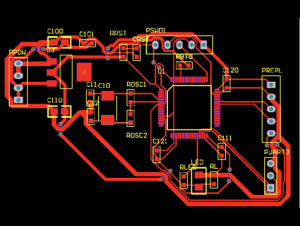
How to Avoid Broken Line Brought DFM (Design for Manufacturing) Question?
Design a complete PCB circuit board , which requires many tedious and complicated processes. Generally , it mainly includes clarifying product requirements, hardware system design, device selection, PCB drawing, PCB production proofing, welding debugging and other steps. Generally, designers have their own design quality checklists, some of which come from the company or department. The other part comes from the specifications of the design and the other part comes from the summary of our own experience. Special inspections include DRC inspection and DFM inspection of the design. These two parts focus on the PCB design output and back-end processing photolithography files. For beginners designing PCB, they often encounter some common low-level problems due to lack of experience and imprecise design. A designed product cannot succeed in one go, it may take several revisions to succeed, and there may be omissions during the revision process. Some common problems ,for example : Broken line. What is a broken line? As the name
the difference between electronic design and PCB design
In the electronic design and manufacturing industry, as well as the field of electronic products, we often hear electronic design and PCB design, sometimes we will equate the two, but they are actually different, let’s take a look at their main differences Electronic Design: PCB Design: Main Differences: Aspect Electronic Design PCB Design Scope Focuses on how the circuit and system work as a whole. Focuses on the physical layout and connection of the circuit on a board. What’s Designed The electrical circuits and how they interact. The physical PCB that holds the components and connects them. Main Activities Circuit design, choosing components, testing functionality. Placing components, routing traces, making sure the board is manufacturable. Tools Used Circuit simulators, system design tools (e.g., SPICE, MATLAB). PCB design software (e.g., Altium, Eagle, KiCad). End Result A circuit diagram (schematic) that shows the design. A PCB layout that’s ready for manufacturing. Electronic
The common material for flexible PCB manufacturing
Flexible PCBs (Printed Circuit Boards) use kinds of materials for their substrates, conductive layers, adhesive, and coverlay. Here are the common materials used, along with some brands and product number: 1. Flexible PCB Substrate Materials(PI, PET) 2. Flexible PCB Conductive Materials 3. Flexible PCB Adhesive Materials 4. Flexible PCB Coverlay The choice of materials depends on the required PCB performance, environmental conditions, and cost considerations. For example, Kapton® PI substrates are commonly used in high-temperature, harsh environments, while PET substrates are more cost-effective for low-end applications. Don’t hesitate to contact us if you have any questions about the flexible circuit. The following shows the performance parameter and datasheets of some material for flex PCB. Click the material name you can see the pdf datasheet. Material for flexible PCBs Recommended max.operating temperature Copper type Tg Ԑr, Dk-Permittivity CTE-z (T<Tg) ElectricStrength Surfaceresistivity Peel strength °C * °C @1MHz ppm/°C KV/mm MΩ
Rigid-Flex PCB Overview
What is Rigid-Flex PCB? Rigid-Flex printed circuit boards (PCBs) are advanced circuit boards that combine the features of both rigid and flexible technologies. They consist of multiple layers of flexible substrates permanently attached to one or more rigid boards. This design allows for both rigid and flexible areas within a single package, making Rigid-Flex PCBs particularly suitable for applications that require space efficiency and durability. These boards are engineered to maintain flexibility, often shaped into specific curves during manufacturing or installation. By leveraging 3D design capabilities, engineers can create complex layouts that maximize spatial efficiency, which is essential in compact electronic devices. Rigid-Flex PCBs offer numerous advantages, including secure connections, dynamic stability, simplified installation, and potential cost savings, making them ideal for various industries, including aerospace, military, and consumer electronics Rigid-Flex PCB Design: Navigating the Challenges Rigid-Flex PCBs combine the advantages of rigid and flexible technologies, offering innovative solutions for
Flexible Printed Circuit Overview
Flexible circuits, commonly known as flex circuits or flexible printed circuit boards (FPC), are crucial components in the world of electronics. Comprising a thin insulating polymer film with conductive patterns, these circuits are often coated for protection. Since their inception in the 1950s, flex circuits have evolved into a vital interconnection technology for advanced electronic products. Unlike traditional rigid PCBs, flexible PCBs are designed to bend, requiring specialized design rules—termed “flex-izing” by the Hemeixin team—to optimize their performance. Typically made from polyimide base material, adhesive layers, and copper traces, flexible PCBs offer significant advantages in weight and assembly efficiency, making them suitable for a variety of applications despite a higher cost compared to rigid PCBs. Their versatility allows them to withstand diverse conditions, catering to industries such as consumer electronics, automotive, and medical devices. With the demand for miniaturized and integrated electronic solutions on the rise, flexible PCBs are increasingly


Wonderful PCB attended the 2024 electronica in Munich, Germany
WonderfulPCB in Electronica 2024 in Munich, Germany The Electronica 2024 exhibition in Munich, Germany, was a major event in the world of electronics, attracting thousands of visitors and exhibitors from around the globe. As one of the largest and most renowned trade shows in the industry, it showcased a wide range of innovations in electronics, including components, systems, and applications across various sectors like automotive, IoT, industrial automation, and more. WonderfulPCB attended the event to showcase their latest PCB technologies, including advances in manufacturing processes, design capabilities, and custom solutions for industries ranging from consumer electronics to automotive. The main exhibition hall was bustling with activity, highlighting cutting-edge trends in PCB production, assembly, and related technologies, such as flexible PCBs, high-frequency circuits, and miniaturization techniques. The exhibition provided an excellent platform for networking, fostering connections between suppliers, manufacturers, and customers, and allowed companies like WonderfulPCB to engage in meaningful

Introduction to Electronic Components
Electronic components refer to parts or devices designed and manufactured based on electronic technology, used to perform specific circuit functions. Semiconductors, typically silicon (Si) or germanium (Ge), possess electrical properties between those of conductors and insulators, allowing for the control of current flow. Electronic components come in various types and can be categorized into three main classes based on their specific functions: passive components, active components, and electronic module devices. Passive components include resistors, capacitors, inductors, and potentiometers, while active components encompass diodes, field-effect transistors (FETs), amplifiers, and logic gates. Although semiconductors are a subset of electronic components, they exhibit distinct characteristics. Semiconductors are typically crystalline materials made from elements such as silicon or germanium, possessing unique electrical properties. In contrast, electronic components are a broad category that includes passive elements, active elements, and electronic modules, which may utilize semiconductor materials but fundamentally control current to achieve specific circuit functions.
What is PCB?
PCB stands for Printed Circuit Board, which is an important electronic component. It serves as a support for electronic components and provides electrical connections, playing a crucial role in the physical support and conduction of electronic devices. Its main function is to enable various electronic components to form circuits and electrical connections according to a pre-designed layout without damage or permanent deformation. PCB are widely used in various electronic devices, including communication equipment, computers, medical devices, and aerospace. The origin of PCB can be traced back to the early 20th century when electronic devices contained many wires that tangled, occupied significant space, and often short-circuited. To solve this problem, German inventor Albert Hanssen pioneered the concept of “wiring” in the early 1900s by cutting conductive paths from metal foil and adhering them to wax paper, creating vias at intersections for electrical interconnections between different layers. This concept laid the theoretical foundation for
Circuit Board’s Main Material: Copper-Clad Laminate
The copper-clad laminate (CCL) comprises a substrate, copper foil, and adhesive. The substrate is an insulating layer board made of polymer synthetic resin and reinforcing materials. A layer of pure copper foil with high conductivity and good weldability is coated on the surface of the substrate, commonly with thicknesses of 18μm, 35μm, or 50μm. CCL with copper foil only on one side of the substrate is called single-sided CCL, while CCL with copper foil on both sides is called double-sided CCL. The adhesive ensures that the copper foil adheres firmly to the substrate. Common thicknesses of CCL include 1.0mm, 1.5mm, and 2.0mm. Types of CCL Common Types and Characteristics of CCL Currently, CCL supplied in the market can be mainly classified into the following types based on the substrate: paper substrate, glass fiber cloth substrate, synthetic fiber cloth substrate, non-woven fabric substrate, and composite substrate. Common Materials for CCL Production
Understanding ODM, OEM, and EMS: Key Manufacturing Models in Electronics and Product Design
01 – ODM ODM (Original Design Manufacturer) refers to a manufacturer that not only produces products but also designs them. Originally, OEMs focused solely on production while design was managed by brand companies. However, as manufacturing alone often yielded low profits, manufacturers began expanding upstream by developing in-house design capabilities. Some Independent Design Houses (IDHs) also moved downstream toward manufacturing, thereby becoming ODMs. Brand owners often choose to work with ODMs to expand product lines quickly, entrusting them with both design and production responsibilities, particularly for lower-end products. Once an ODM develops a product, other brands may request production under their own branding. Whether an ODM can produce the same design for third parties depends on whether the branding client has exclusive rights to the design. Today, ODMs offer an integrated solution with design, production, and sourcing capabilities for brand companies. 02 – OEM OEM (Original Equipment Manufacturer) is typically defined as
Differences and characteristics of analog and digital signalsdigital signals
Differences and characteristics of analog and digital signals In electronics, signals can be divided into two types: analog signals and digital signals. They have obvious differences and characteristics in terms of transmission methods, processing methods, accuracy, noise, etc. The following will introduce the differences and characteristics of analog and digital signals from these aspects in detail. First, the difference between analog and digital signals 1. Different transmission methods: analog signals are continuous signals, which can be transmitted through analog transmission; digital signals are discrete signals, which are usually transmitted through digital transmission. 2. different processing: analog signal processing is usually through the analog circuit, such as amplification, filtering, regulation, etc.; digital signal processing is usually through the digital circuit, such as coding, decoding, calculation, etc.. 3. Different precision: the precision of analog signals is usually affected by noise and interference, limited precision; the precision of digital signals is usually determined
Introduction to Common PCB Manufacturing Files
Introduction to Common PCB Manufacturing Files When designing and manufacturing printed circuit boards (PCBs), choosing the right manufacturing file format is critical. Different formats offer a variety of features, benefits and limitations. The following is an introduction to four common PCB manufacturing file formats: Gerber, ODB++, IPC-2581, and Gerber X2. 1. Gerber File Gerber files are a standard format for describing the various layers of a PCB, such as copper, pad protection, and screen printed layers. Developed by Gerber Systems Corp. these files are critical for communicating designs to PCB manufacturers. Benefits: Compatibility: Universally applicable as it is compatible with most PCB design and manufacturing tools. Long history: known and widely used in the industry for a long time. Disadvantages: Limited metadata: the original format lacks detailed metadata, which can lead to some ambiguity. File complexity: multiple files are required to represent different layers, which is more complicated to manage.