

PCB Pad Design Issues Explained
The assembly quality of SMT (Surface Mount Technology) is directly related to the PCB pad design, and the size ratio of the pads is crucial. If the PCB pad design is correct, minor misalignment during placement can be corrected during the reflow soldering process (known as self-alignment or self-correction effect). On the other hand, if the PCB pad design is incorrect, even precise placement can result in component misalignment, solder bridges, and other soldering defects after reflow soldering. Basic Principles of PCB Pad Design Based on the analysis of various component solder joint structures, to ensure the reliability of the solder joints, the PCB pad design should focus on the following key factors: Solderability Defects Caused by Pad Size Inconsistent Pad Sizes Pad sizes must be consistent, and their length should be within an appropriate range. Pads that are too short or too long can cause the “tombstoning” (standing up)

How to Avoid Pitfalls in PCB Hole and Slot Design
In the design of electronic products, from creating the schematic to PCB layout and routing, various errors can occur due to a lack of experience or knowledge, which can hinder progress and, in severe cases, render the circuit board unusable. To prevent such issues, it is essential to improve our understanding of this area and avoid common mistakes. This article will discuss some common drilling issues during PCB design to help you avoid repeating the same mistakes. Drilling can be categorized into three types: through-hole, blind hole, and buried hole. Through-holes include plated through holes (PTH), non-plated through holes (NPTH), and vias, all of which serve to provide electrical connectivity between layers. Regardless of the type, missing holes can lead to significant functional failures, making correct drilling design crucial. Problem 1: Slot Holes Placed on the Wrong Layer in Altium Design Problem 2: Zero-Diameter Holes in Altium Design Problem 3:

Do You Understand the Four Major PCB Testing Methods?
A PCB (Printed Circuit Board) is an essential electronic component, often referred to as a printed circuit or printed wiring board. The quality of the PCB largely determines the performance of electronic components, making testing a critical part of the PCB production process. Testing typically identifies functional defects, such as opens, shorts, and other issues that are not easily visible. To ensure the success of any product design, multiple rounds of testing are necessary. PCB testing helps minimize major issues, identify smaller errors, save time, and reduce overall costs. PCB testing is mainly used to address potential problems during the manufacturing and final production stages. These tests can also be applied to prototypes or small-scale assemblies to identify potential issues with the final product. Testing Methods for Bare PCB 1. AOI Testing (Automatic Optical Inspection) AOI equipment is widely used across various industries, including PCB manufacturing, as a key quality assurance
8 Safety Distances That Must Be Considered in PCB Design
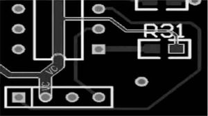
There are many safety distance considerations in PCB design, including spacing between traces, character spacing, pad spacing, and more. Here, we classify them into two categories: electrical-related safety distances and non-electrical-related safety distances. 01 Electrical-Related Safety Distances Trace-to-Trace Spacing For the processing capabilities of mainstream PCB manufacturers, the minimum distance between traces should not be less than 0.075mm. The minimum trace spacing refers to the smallest distance between a trace and another trace or between a trace and a pad. From a manufacturing perspective, larger trace spacing is better. A more common value is 0.127mm. Pad Hole Diameter and Pad Width For mainstream PCB manufacturers, if the pad uses mechanical drilling, the minimum hole diameter should not be less than 0.2mm. If laser drilling is used, the minimum hole diameter should not be less than 0.1mm. The hole diameter tolerance may vary slightly depending on the material, but it is
Reliability Analysis of Hole Spacing in PCB Design
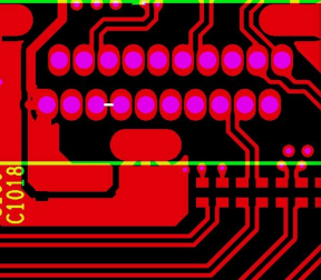
The production of single-sided or double-sided PCBs typically involves drilling non-conductive or conductive holes directly after the material is cut, while multi-layer boards are drilled after the lamination process. Holes are categorized based on their function, including component holes, tool holes, through holes (Vias), blind holes, and buried holes (blind and buried holes are a type of via hole). Conventional drilling is done using mechanical drilling equipment. In actual manufacturing, the spacing between holes usually impacts both the machining process and the final product’s reliability. Hole Spacing Manufacturing Requirements: Via Holes (Conductive Holes): Pad Holes (PTH): Non-Plated Holes and Slots (NPTH): Reliability Impact of Hole Spacing: Hole-to-Hole Spacing: This refers to the distance from the inner wall of one hole to the inner wall of another, not the distance between the pads. It’s crucial to distinguish between these measurements. If the hole-to-hole spacing is too small, what are the potential

PCB Manufacturability Design and Case Analysis: Silkscreen, Outline, and Panelization
PCB design is a complex process that involves various unforeseen factors that can impact the overall outcome. To ensure high-quality PCB production on time—without extending design time or incurring costly rework—design and circuit integrity issues must be identified early in the process. However, there are many minor details in PCB design that, if overlooked, can significantly affect the PCB’s performance and even determine the product’s success or failure. To maximize design efficiency and product quality, what additional details should we focus on? Through practical experience working with customers, we’ve summarized key considerations for silkscreen, outline, and panelization design. As a high-reliability multilayer PCB manufacturer, Wonderful PCB specializes in PCB R&D and manufacturing, delivering high-reliability and fast-turnaround prototyping experiences. Our mission, “Lower Costs and Improve Efficiency for the Electronics Industry,” reflects our understanding that design development and engineering costs, while a small percentage of the production chain, can have a significant
PCB Manufacturability Design and Case Analysis: Holes and Slots
Vias are an unavoidable aspect of PCB design. During the layout process, avoiding all crossover lines is often challenging. To resolve this, vias are used to achieve interlayer connectivity, leading to the development of double-sided and multilayer PCBs. Consequently, vias have become a critical element of PCB design. From a design perspective, vias serve two main purposes: electrical connection and mechanical support or positioning. These roles fulfill electrical requirements or physical needs. Therefore, vias are often classified further into electrical vias and mechanical support holes, with the latter divided into solder pad holes (typically plated) and mounting holes (often non-plated). A via mainly consists of two parts: Pad area: The area surrounding the drill hole. In high-speed, high-density PCB designs, designers typically aim for the smallest possible vias to maximize routing space and minimize parasitic capacitance, making them more suitable for high-speed circuits. However, reducing via size increases manufacturing costs
Manufacturability Design for PCB Inner Layers
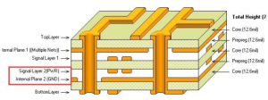
When a PCB engineer lays out a product, it involves more than just component placement and routing. Designing the power and ground planes in the inner layers is equally critical. Managing inner layers requires consideration of power integrity, signal integrity, electromagnetic compatibility, and Design for Manufacturability. Difference Between Inner Layers and Outer Layers Outer layers are used for routing and soldering components, while inner layers are dedicated to power and ground planes. These layers are only present in multilayer boards, where they provide pathways for power and ground. Common designs, such as double-layer, four-layer, and six-layer boards, refer to the number of signal layers and internal power/ground layers. Inner Layer Design 1. Ground Layer Under Critical Signals For high-speed, clock, and high-frequency signals, placing a ground layer directly beneath these signals minimizes loop path length and reduces radiation. 2. Power Plane and Ground Plane Area In high-speed circuit design, power plane radiation

Key Points of PCB Stamp Hole Bridge Design
Typically, PCB uses V-CUTs. Stamp holes are more likely to be used when dealing with irregular or circular boards. Stamp hole bridges connect boards (or empty boards) primarily to provide support, ensuring the boards do not separate during processing. This also prevents mold collapse during molding. Stamp holes are most commonly used to create independent PCB modules, such as Wi-Fi, Bluetooth, or core board modules, which can be used as independent components mounted on another PCB during the assembly process. Bridge Distance and Width Stamp Hole Design Stamp Hole Bridges + V-CUT Peripheral Half-Hole Boards with Stamp Holes Special Notes This approach ensures structural integrity, ease of processing, and reliability during PCB assembly.
Importance of PCB Layout about Electronic Components in PCBA
Proper installation of electronic components on the PCB is crucial to reducing soldering defects. When arranging electronic components, avoid areas with high deflection values and high internal stress. Distribute components evenly, especially those with high thermal conductivity. Avoid using oversized PCBs to prevent expansion and contraction. Poor PCB layout design can affect the PCB’s manufacturability and reliability. Many designers, aiming to maximize the utilization of the circuit board space, place components as close to the edges as possible. This practice can create significant challenges for manufacturing and PCBA assembly, even making soldering assembly impossible. Impact of Edge Component Layout: 1.Board Edge Milling: Components placed too close to the board edge may have their pads milled off during shaping. Generally, the pad-to-edge distance should be greater than 0.2mm. Otherwise, the pads on the board edge components may be milled off, making subsequent assembly impossible. 2. Board Edge V-CUT: If the board edge

How to Prevent Solder Mask Omission in PCB Design
The solder mask layer on a PCB refers to the part of the board covered with green solder resist ink. Areas with solder mask openings are left without ink, exposing the copper for surface treatment and soldering components. Areas without openings are covered with solder mask ink to prevent oxidation and leakage. Three Reasons for Solder Mask Openings: 1. Through-Hole Pad Openings: Through-hole pads require solder mask openings. Without these openings, the soldering points will be covered by ink, making it impossible to solder component leads. 2. SMD Pad Openings: Solder mask openings are required for SMD pads to allow soldering. If the soldering area lacks openings, the pads will be covered by ink, effectively rendering them unusable. 3. Large Copper Area Openings: To increase current capacity without widening traces, certain areas are tin-plated. Tin-plating requires solder mask openings in these areas. Why Solder Mask Openings Are Larger Than Pads Solder mask openings
Entire Process of Gold Finger PCB in Design and Manufacturing
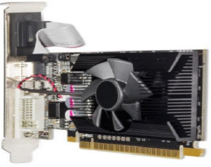
In computer memory modules and graphics cards, there is a row of golden conductive contact pads, commonly known as “gold fingers.” In the PCB design and manufacturing industry, the PCB gold finger (Gold Finger or Edge Connector) refers to the connector used as the external interface for the PCB to connect to external devices. In this article, we will explore the design of the “gold finger” in PCB and discuss some key manufacturing considerations. Functions and Applications of Gold Finger Interconnect Point for Gold Finger When auxiliary PCBs (such as graphics cards or memory modules) connect to a motherboard, they do so through a slot, such as PCI, ISA, or AGP. The gold finger serves as the interconnection point, allowing the transmission of signals between the peripheral devices or internal cards and the computer. Special Adaptors, Gold fingers, can enhance the functionality of a motherboard by allowing a secondary PCB
Assisting BOM Error Checking to Support Component Procurement
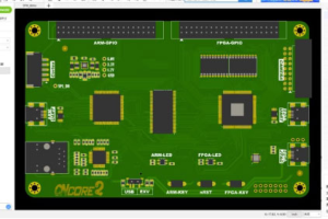
The Bill of Materials (BOM) for electronic products is a straightforward yet intricate task. With numerous components, even a minor oversight can lead to procuring the wrong components. Manual matching increases the risk of errors. If mistakes occur during the BOM matching stage, subsequent procurement inquiries and customer quotes are likely to be flawed as well. Currently, there is no unified component database in the industry. Engineers often build their own commonly used packaging libraries, resulting in inconsistent component information. The primary reasons are as follows: During the design process, electronic engineers focus on the electrical parameters of components. However, in the production and procurement process, personnel need to pay attention to other information, such as the manufacturer, supplier, and manufacturer part number (MPN). The BOM provided by customers may contain hundreds or even thousands of line items with uncertain formats and columns. Generally, customers provide at least an original
8 Safety Distances to Consider in PCB Design
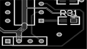
PCB design requires attention to numerous safety distances, including trace spacing, text spacing, and pad spacing. These considerations can generally be categorized into two types: electrical safety distances and non-electrical safety distances. 01 Electrical Safety Distances Trace-to-Trace Spacing For mainstream PCB manufacturers, the minimum spacing between traces must not be less than 0.075mm. The minimum trace spacing refers to the smallest distance between traces or between a trace and a pad. From a production perspective, larger spacing is better, with 0.127mm being a common standard. Pad Hole Diameter and Pad Width If the pad uses mechanical drilling, the minimum hole diameter should be no less than 0.2mm; for laser drilling, the minimum hole diameter is 0.1mm. The hole diameter tolerance varies slightly depending on the material, typically controlled within 0.05mm, and the minimum pad width should not be less than 0.2mm. Pad-to-Pad Spacing The minimum spacing between pads must not
How to avoid pitfalls in square slots and square holes of device pins
Introduction Nowadays, circuit boards use more SMD components than plug-in components, but for those electronic products with higher heat dissipation requirements, the performance of plug-in components will be better than that of SMD components. In addition, the external interface of the motherboard and the devices of the connector all use plug-in pins, such as USB, HDMI, network ports, and other devices.Regarding the square pins of plug-in devices, there are manufacturability issues in DFM analysis. Device pins are generally round or oval, but the pins of some pin header devices are square. Square pins are not very convenient when making packages, even if some EDA software can make packages with square pins. However, square pin holes cannot be made on the manufacturing side because the drilling tip is round. Square Pin Drawing Method 1. Allegro draws square pins First, open the Padstack Editor package drawing tool. During the package drawing process,
All the BGA welding problems you want to know are here
BGA Overview BGA is a type of chip package, short for Ball Grid Array in English. The package pins are ball grid arrays at the bottom of the package, and the pins are spherical and arranged in a grid-like pattern, hence the name BGA.Many motherboard control chips use this type of packaging technology, and the materials are mostly ceramic. Memory packaged with BGA technology can increase the memory capacity by two to three times without changing the volume. Compared with TSOP, BGA has a smaller volume, better heat dissipation, and electrical performance. BGA Package Pad Routing Design 1. Routing between BGA pads During the design, the BGA pad spacing is less than 10mil, and routing is not allowed between two BGAs, because the line width spacing of the routing exceeds the production process capability. If routing is to be done, the BGA pad can only be reduced. When making the production
The pitfalls that must be mentioned about DIP devices
DIP Overview DIP is a plug-in. The chip using this packaging method has two rows of pins, which can be directly soldered on a chip socket with a DIP structure or in a soldering position with the same number of solder holes. Its characteristics are that it can easily realize the perforation soldering of the PCB board and has good compatibility with the motherboard. However, due to its large packaging area and thickness, and the pins are easily damaged during the plug-in and unplug process, the reliability is poor. DIP is the most popular plug-in package, and its application range includes standard logic IC, memory LSI, microcomputer circuits, etc. Small outline package (SOP). Derived SOJ (J-type pin small outline package), TSOP (thin small outline package), VSOP (very small outline package), SSOP (shrink SOP), TSSOP (thin shrink SOP) and SOT (small outline transistor), SOIC (small outline integrated circuit), etc. DIP device
Easy to use! No need to worry about PCB graphic alignment
Many friends will encounter the situation of graphic misalignment when using wonderfulpcb DFM Services software to import Gerber files. The reason for the misalignment of graphics is that there are unknown objects outside the design file frame, and the canvas size of each layer is different, which causes the coordinates to change with the canvas size when the EDA software converts the Gerber file, resulting in graphic offset. So how to align the graphics of the Gerber file? The following wonderfulpcb DFM Services takes you to fly! Board layer graphic alignment 1. Single layer alignment The first step is to close other layers and only display the layer to be moved and the reference alignment layer. Double-click the layer to close other layers, display only one layer, and then click to open another layer. The second step is to open the grab center, that is, to grab the center of the graphic

PCB Design Pitfall Avoidance Guide
Ensuring the reliability of electronic product designs is crucial. Manufacturability design encompasses three key aspects: PCB manufacturability design, PCBA assembly design, and cost-effective manufacturing design. Among these, PCB manufacturability design focuses on the manufacturing perspective of PCB boards, considering process parameters to improve production yield and reduce communication costs. Design considerations include line width and spacing, hole-to-line and hole-to-hole distances, all of which must be addressed during the design phase. The Importance of PCB Design In electronic product development, the PCB serves as the physical medium for the design content, realizing all design intentions and product functions. Therefore, PCB design is an indispensable link in any project. Manufacturability design of PCBs requires engineers’ attention to ensure that the design aligns with manufacturing capabilities. Common Design Pitfalls After completing PCB design, the physical circuit board is produced. Often, the designed PCB cannot be manufactured due to mismatches between the design process

What files of PCB can be used for DFM Analysis?
Why do PCB design need assembly analysis? It is to consider PCB assembly in the early design stage to get the best product.There is a common problem that may be less common among PCB design masters, but it is still common for novices, that is, the initial circuit board design does not fully consider the assembly. On the contrary, more attention is paid to the PCB itself, and there is no extensive understanding of the problems in the manufacturing process, which leads to product design failure. The following is an introduction to the data files that need to be prepared before assembly analysis! 1. PCB/ODB files 1) PCB file: First open the DFM software, click “File” to find the file to be used, click Open and wait for the software to automatically parse it before using it. Or open the software and drag the file into the software graphics window