PCB Surface Finish Process
01 What is PCB surface treatment process? Copper surfaces on PCB without solder mask coverage, such as solder pads, gold fingers, mechanical holes, etc. If there is no protective coating, the copper surface is easily oxidized, which affects the soldering between bare copper and components in the solderable area of the PCB. As shown in the figure below, the surface treatment is located on the outermost layer of the PCB, above the copper layer, serving as a “coating” on the copper surface. The main function of surface treatment is to protect the exposed copper surface from oxidation circuits, thereby providing a solderable surface for soldering during welding. 02 Classification of PCB surface treatment processes PCB surface treatment processes are divided into the following categories: Hot air solder leveling (HASL) Tin immersion (ImSn) Chemical nickel gold (immersion gold) (ENIG) Organic Solderable Preservatives (OSP) Chemical Silver (ImAg) Chemical nickel plating, chemical palladium plating,

National Day Holidays 2024
Wonderful Group will have our National Day holiday from 1st to 6th
What is a Rigid-Flex PCB?
A rigid-flex PCB is a new type of printed circuit board that combines the durability of rigid PCB and the flexibility of flexible PCB (FPC). Among all types of circuit boards, rigid-flex PCB offer the strongest resistance to harsh environments, making them popular among manufacturers of industrial control, medical, and military equipment. WonderfulPCB is also gradually increasing the proportion of rigid-flex PCB in its total production. The advantages of rigid-flex PCB are their excellent properties from both rigid PCB and flexible FPCs. They can be folded, bent, and save space, while still allowing the complex welding of components. Compared to traditional cables, they offer longer lifespan, more reliable stability, and are less prone to breaking, oxidation, or detachment, greatly improving product performance. However, rigid-flex PCB have some drawbacks: their production involves numerous processes, they are difficult to manufacture, have a low yield rate, require a large amount of material and labor, making them expensive and with a
SMT Processing in Electronics Manufacturing
SMT (Surface Mount Technology) processing is a crucial technique in the manufacturing of electronic devices. For procurement personnel new to this field, understanding the process flow of SMT assembly is fundamental. This article outlines the main steps in SMT processing to help you quickly grasp the core aspects of this technology. Basic Concept of SMT Processing SMT processing involves directly mounting electronic components onto the surface of printed circuit boards (PCBs) and soldering them using methods such as reflow soldering or wave soldering. Compared to traditional through-hole technology, SMT offers advantages like higher assembly density, smaller size, lighter weight, greater reliability, and higher production efficiency, making it widely used in modern electronics manufacturing. The SMT processing workflow mainly includes the following steps: PCB Design and Fabrication The first step in SMT processing is designing and fabricating a PCB that meets the requirements. PCB design must consider component layout, routing, and
FPC Cutting
1. FPC Material Cutting Except for certain materials, most of the materials used in flexible printed circuits (FPC) come in rolls. Since not all processes require roll-based techniques, some processes, such as drilling metallized holes in double-sided flexible PCB, must be done with sheet-form materials. The first step for double-sided flexible PCB is cutting the material into sheets. Flexible copper-clad laminates have very low tolerance to mechanical stress and can be easily damaged. Any damage during the cutting process can significantly affect the yield of subsequent processes. Therefore, although cutting may seem simple, great care must be taken to ensure the material quality. For small quantities, manual cutting machines or rotary cutters can be used. For large-scale production, automatic cutting machines are preferable. Whether it’s single-sided or double-sided copper-clad laminates or cover films, cutting precision can reach ±0.33 mm. The cutting process is highly reliable, and the cut material is automatically
Classification of PCB
PCB (Printed Circuit Board) is an important electronic component that serves as a support structure for electronic components and a carrier for electrical connections. It is called a “printed” circuit board because it is produced using electronic printing techniques. PCB are one of the essential components in the electronics industry. Almost every electronic device, from small items like digital watches and calculators to large systems like computers, communication electronics, and military weapon systems, uses printed circuit boards to connect integrated circuits and other electronic components electrically. A printed circuit board consists of an insulating substrate, connecting wires, and pads for assembling and soldering electronic components, serving both as conductive pathways and an insulating base. It can replace complex wiring to achieve electrical connections between various components, simplifying assembly and soldering processes, reducing the workload associated with traditional wiring methods, and significantly decreasing labor intensity. Additionally, PCB help reduce the overall size of devices,
What is the PCB Fabrication Process?
What is the PCB Fabrication Process? As the carrier of electronic components, PCB plays a vital role in the electronics manufacturing industry. Its production process is complex and precise, directly affecting the performance and quality of the final product. WonderfulPCB, a trusted SMT processing factory, provides a detailed analysis of the PCB production process to help electronics manufacturers and procurement teams better understand it. Overview of the PCB Production Process The PCB production process can be divided into several key stages: inner layer fabrication, lamination, drilling, metallization, outer layer fabrication, surface protection, and final inspection and packaging. Each step involves various techniques and technologies, requiring a high degree of precision and expertise. Inner Layer Fabrication The inner layers are the core of the PCB, connecting the electronic components. The process includes: Board Cutting: Cutting the original PCB substrate to the required size for production. Pre-treatment: Cleaning the substrate surface to
What is the methods of PCB Assembly?
PCBA Assembly Methods: SMT and DIP PCBA (Printed Circuit Board Assembly) processing involves a complete set of steps including PCB manufacturing, SMT (Surface Mount Technology) processing, DIP (Dual In-line Package) insertion, quality inspection, testing, and assembly to form a finished electronic product. This process is referred to as PCBA processing, and the resulting circuit board after processing is called a PCBA. There are various types of PCBA, and several assembly methods used in PCBA processing. Below, WonderfulPCB, a professional PCBA factory, provides a brief introduction to some common assembly methods. Single-Sided Hybrid Assembly This assembly method uses a single-sided PCB. In a single-sided hybrid assembly, SMT components and DIP components are distributed on different sides of the PCB. The soldering side is isolated to one side, and the SMT components are placed on the other side. This method employs single-sided PCB and wave soldering technology. There are two specific assembly
Summary of key points in power PCB design
Power PCB design is a key link to ensure efficient and stable operation of electronic equipment. The following is a detailed summary of the key points of power PCB design: Heat dissipation design: Design appropriate heat dissipation structures, such as heat sinks, heat pipes, etc., to improve the heat conduction efficiency. Copper foil layout: Increase the copper foil area of PCB to improve thermal conductivity and reduce the resistance of copper foil. Thermal isolation: Set a thermal isolation belt between high-heat devices and sensitive components to reduce thermal effects. Decoupling capacitor: Place appropriate decoupling capacitors on the power line to filter out high-frequency noise. Multi-power layer: In multi-layer board design, use a dedicated power layer and ground layer to improve the stability of power supply. Ground plane: Use ground plane in multilayer boards to provide low-impedance ground loops. Partition ground: For high-frequency or high-speed signals, use partition ground design to
A detailed explanation of the seven major application circuit designs of op-amps
Basic analysis method for op amps: virtual open circuit, virtual short circuit. For unfamiliar op amp application circuits, use this basic analysis method. Op amps are widely used devices. When connected to appropriate feedback networks, they can be used as precision AC and DC amplifiers, active filters, oscillators, and voltage comparators. The figure above is a typical active filter circuit (Saron-Kayl circuit, a type of Butterworth circuit). The advantage of active filtering is that it can make signals greater than the cutoff frequency decay more quickly, and the filtering characteristics do not require high capacitance and resistance. The design points of this circuit are: under the condition of meeting the appropriate cutoff frequency, the resistance values of R233 and R230 should be selected as consistent as possible, and the capacitance of C50 and C201 should be selected as consistent (when the resistance and capacitance values of the two-stage RC circuit

Dragon Boat Festival Holiday Notice – 2024
Dear Valued Customers, We hope this message finds you well. As the Dragon Boat Festival approaches, we would like to inform you of our holiday arrangements: We appreciate your understanding and cooperation. Should you have any urgent matters, feel free to reach out to us before the holiday period. Welcome to China to experience the Dragon Boat Festival Best regards, Wonderful Group

Summary of Power Manager Unit PCB Design Considerations
Power Management Units (PMUs) are crucial components in portable electronic devices, integrating multiple functionalities into a compact package to enhance system efficiency and energy conservation. As the core of the power system, PMU PCB design directly impacts the performance and stability of electronic systems, especially in complex applications with stringent performance requirements. 1. Key Features of PMUs 2. Typical Components of a PMU 3. PMU Module Layout Considerations 4. PMU Module Routing Considerations 5. Conclusion An in-depth analysis of PMU module layout and routing reveals the crucial role of optimized design in performance enhancement. Meticulous attention to detail is essential for securing a product’s position in the competitive market. As technology advances, innovation will continue to open new avenues and challenges in PMU design. Let’s work together to explore the vast potential of power management and provide robust support for the reliable and long-lasting operation of electronic devices. I hope

Power Supply Unit Design Fundamentals: Inductor Behaviour in a Switching Power Supply
Introduction In this introductory article, we’re going to talk about the action of an inductor in a switch mode power supply. If you’re new to power supply design and you’re wondering why a diode seems to be forward-biased while it looks like it shouldn’t be, then in all likelihood, that is because of the inductor. This article is for you. Understanding Inductors Initially, we studied inductors at university, both in AC and DC circuits. In an AC circuit, we give the inductor a sinusoidal input and observe changes in amplitude and phase. In a DC circuit, we provide a unit step input and study the resulting changes in current or voltage across the inductor. However, the behavior of an inductor in a switch mode power supply differs significantly from the simple AC or DC circuits studied in university. Basic Inductor Principles An inductor always tries to maintain the current flowing

Choosing the Right Power Supply Design Service Provider: A Guide for Customers
When it comes to selecting a power supply design service provider, making the right choice is paramount for the success of your project. Here’s a comprehensive guide to help you evaluate their services and capabilities effectively: 1. Experience and Expertise: 2. Technical Competence: 3. Portfolio and References: 4. Customization and Flexibility: 5. Collaboration and Communication: 6. Design Tools and Resources: 7. Quality Assurance Processes: 8. Compliance and Certification: 9. Cost and Timelines: 10. Customer Support and After-Sales Service: By carefully evaluating these factors, you can select a power supply design service provider that aligns with your project needs and delivers high-quality, reliable solutions to help you achieve your objectives.

Power supply PCB design checklist
By following these checklists, hardware engineers can ensure the successful design and implementation of power supply PCBs that meet performance, reliability, and safety requirements.

PCB Layout Review Checklist
Top 14 points of the PCB Layout checklist Top 14 points of the PCB Layout checklist 1. Common practices When designing PCB, to make the design of high-frequency circuit boards more reasonable and have better anti-interference performance, the following aspects should be considered:(1) Reasonably select the number of layers. When wiring high-frequency circuit boards in PCB design, use the middle inner plane as the power and ground layer, which can play a shielding role, effectively reduce parasitic inductance, shorten the length of signal lines, and minimize signal cross-interference between.(2) Wiring method: The wiring must be turned at a 45° angle or in an arc, which can reduce the emission of high-frequency signals and their coupling.(3) Trace length: The shorter the trace length, the better, and the shorter the parallel distance between two lines, the better.(4) Number of via holes: The fewer the number of via holes, the better.(5) Interlayer wiring
How to Quickly Design the Layout of an LDO Power Module
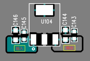
In today’s world, where electronic devices are omnipresent, the design and application of power modules have become central to electronic engineering. The Low Dropout (LDO) linear regulator power module is particularly valued for its superior linear characteristics and stability. To meet the increasing performance demands of modern electronics, optimizing the PCB design of LDO power modules for higher efficiency and stability is a critical task for engineers. Understanding LDO LDO regulators play a crucial role in power supply design by maintaining a small voltage difference between input and output, which enhances linear voltage regulation efficiency. The dropout voltage is the minimum difference between the input and output voltage where the regulator can still maintain a regulated output. This dropout voltage can vary with changes in the load. Characteristics of LDO Linear Regulated Power Supply LDO linear regulators are popular due to their excellent performance, high reliability, ease of assembly and
Wonderful PCB in Global Sources Hong Kong Consumer Electronics Trade Show 2024
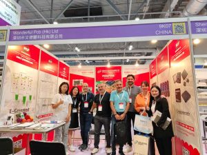
WonderfulPCB proudly attended this year’s Global Sources Hong Kong Consumer Electronics Trade Show, one of the leading events in the electronics industry. We showcased our capabilities in PCB manufacturing, PCBA assembly, and electronic design, emphasizing our commitment to quality and innovation. The exhibition provided an excellent platform to connect with global industry professionals, explore cutting-edge technologies, and gain valuable insights into market trends. Our team engaged with numerous potential clients, discussing customized solutions to meet diverse requirements and highlighting our advanced SMT production lines, comprehensive supply chain, and design expertise. The positive feedback we received reinforced our dedication to delivering exceptional products and services. Participating in this event not only enhanced our visibility in the market but also opened new doors for collaborations, making it a significant milestone in our journey of growth and excellence.

the Labor Day holiday – 2024
the Labor Day holiday – 2024 Dear Customers, We want to inform you that our company will be observing the Labor Day holiday. The holiday period will be from May 1st to May 5th, 2024. We will resume work on May 6th, 2024. Please prearrange any urgent requests to help us provide the best service possible during this time. If you have any emergencies during the holidays, please call us at +86 19129538762 or email us at [email protected]. Thank you for your trust and support all the time, we will do our best to provide quality products and services With Best Regards Wonderful Group