PCB Silkscreen are also known as “silk screen” in the industry. PCB silk screen can be seen on general PCB boards, so what are the functions of PCB silk screen?
1. Identifying Electronic Components
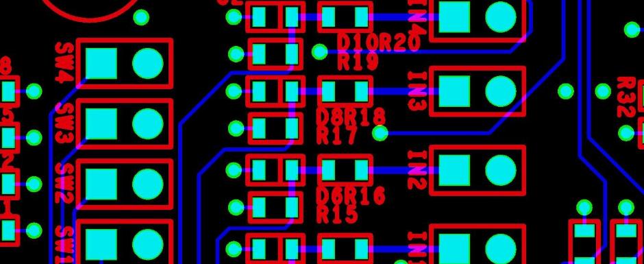
As we all know, there are countless electronic components. The silk screen Silkscreens on the PCB board are used to identify which electronic components are placed on each pad.
2. SMT Assembly
SMT assembles patches through silk screen Silkscreens. PCB silk screen Silkscreens help the factory identify the position numbers of each component during the patching process.
3. Product Repair
PCB silk screen Silkscreens are also helpful for product repairs. They guide the repair personnel in locating the corresponding position of each component.
4. Product Identification
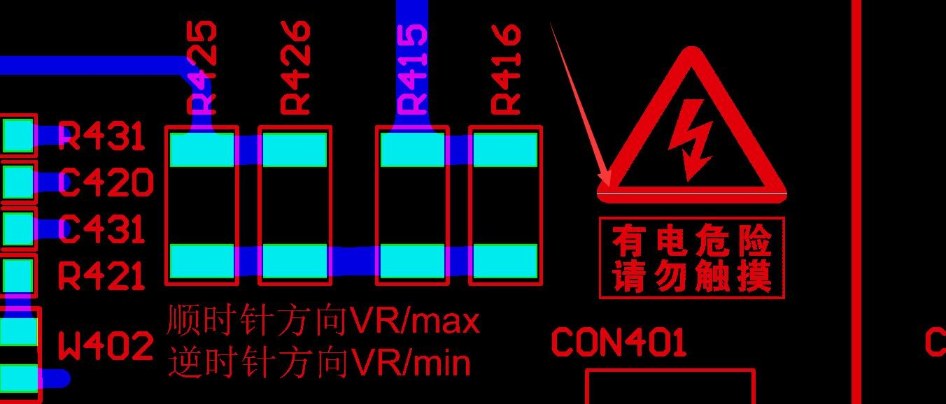
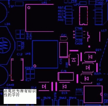
In addition to component identification, PCB silk screen Silkscreens can include other essential information, such as product name, manufacturer logo, UL marks, production cycle codes, and other identification codes.
DFM Design of PCB Silkscreen
Engineers primarily focus on power integrity and signal integrity during the layout process. However, the manufacturability of Silkscreens is often overlooked. For example, Silkscreens may overlap with solder pads, which can complicate PCB continuity tests and component soldering. If Silkscreen design is too small, it can lead to difficulties in screen printing; if too large, Silkscreens can overlap and become hard to distinguish.
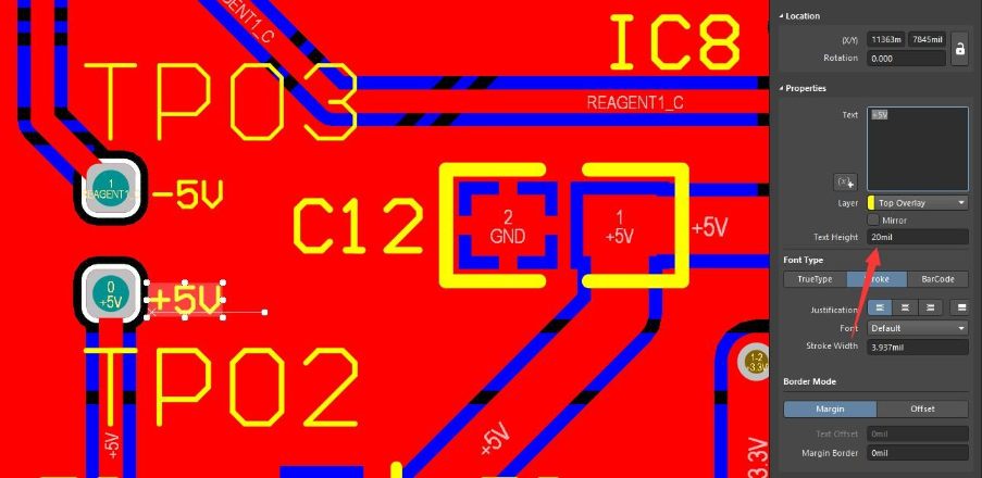
1. The Distance Between the Silk Screen and the Pad
Silk screen Silkscreens need to be 3-6 mils away from the solder mask window pad because there are always deviations during the silk screen printing process. If silk screen Silkscreens are printed on the pad, they must be moved to avoid affecting welding quality, and potentially making the pad unsolderable.

2. Silk Screen Line Width
The line width refers only to the thickness of the individual lines of the Silkscreens, not the total width of the entire Silkscreen. If the line width is too small, the ink cannot be deposited properly, leading to an incomplete or missing silk screen Silkscreen.

3. Linear White Ink Block
If a silk screen Silkscreen consists of lines, an insufficient line width can cause the Silkscreen to appear as a large block. During the photo drawing process, the line width will be too ll to create a proper image, resulting in the whole silk screen being omitted.
4. Silk Screen Silkscreen Spacing
Silkscreen blurring can occur for two reasons: the Silkscreen line width is too thick or the spacing between Silkscreens is too small. In either case, the Silkscreens will merge into a lump, causing them to appear blurry and indistinct.
5. Silk Screen Silkscreen Height
Silkscreen height refers to the total height of a Silkscreen. The minimum height limit is 25 mils. If the Silkscreen height is less than 25 mils, the silk screen will not be clear, and the Silkscreens may appear as a solid block of ink.
6. Unclear Silk Screen Markings
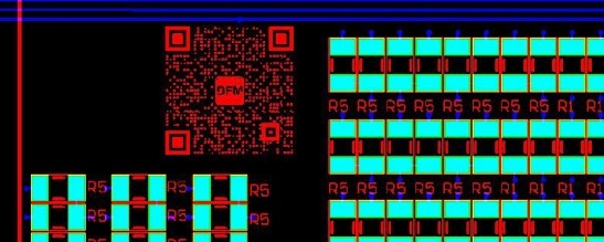
When designing QR codes or barcodes on the PCB, special care must be taken to consider the production capability. If the gap between elements is too small, the silk screen may blur, making QR codes or barcodes unreadable and preventing scanning.
PCB Silkscreen Production Process
PCB Silkscreen are typically white, black, or yellow. The color selection depends on the color of the solder mask. For example, if the solder mask is black, green, or blue, white ink is used for the Silkscreens. If the solder mask is black oil, black ink is also used for the Silkscreens, as using the same color would make the Silkscreens hard to recognize.
1. Silkscreen Production Capacity
The ability to produce silk screen Silkscreens is also related to the copper thickness. Thicker copper requires higher Silkscreen requirements because the copper foil may have height differences where it intersects with the substrate. These uneven areas can cause blurred silk screen printing.
- When the base copper thickness is 12-18 µm, the minimum line width is 4.5 mils, and the minimum Silkscreen height is 25 mils.
- When the base copper thickness is 35 µm, the minimum line width is 5 mils, and the minimum Silkscreen height is 30 mils.
- When the base copper thickness is 70 µm, the minimum line width is 6 mils, and the minimum Silkscreen height is 45 mils.
- For negative Silkscreens (reverse effect), the minimum line width is ≥8 mils, and the minimum ink width is >5 mils.
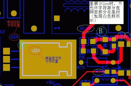
2. Silkscreen Processing on the Pad
Silkscreens should be moved off the pad to ensure the board’s solderability. When adjusting or moving Silkscreens, it is important not to alter the polarity of the Silkscreen frame, as this could reverse the polarity of the components.
3. Avoiding Incomplete Silkscreens
For large tin (or gold) surface pads, try to move Silkscreens instead of cutting them, to maintain clear identification. Alternatively, allow the Silkscreens to remain on the tin or gold surface, and ensure that the process applies tin or immersion gold first, followed by silk screening of the Silkscreens.
4. Silkscreen Positive and Negative Processing
Top-layer Silkscreens should display as positive, while bottom-layer Silkscreens should display as reverse (negative). If these conditions are not met, mirror processing is required. For example, if the bottom layer Silkscreens are positive, they should undergo mirror processing to avoid reversed Silkscreens in the final PCB.
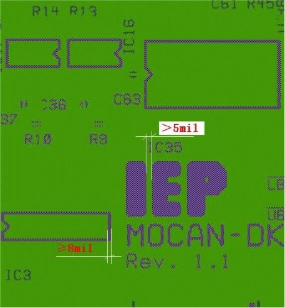
5. Negative Film (Negative Silkscreen) Processing
When designing negative Silkscreens, the ink cannot be placed on pads or into holes. The solder mask white oil block should be 10 mils or more on one side. For vias, the cover oil should be 4 mils or more on one side. The spacing between Silkscreens should be greater than 5 mils, and the line width should exceed 8 mils.
6. Logo and Identification Code Addition
When ordering PCB manufacturing and needing to add identification codes (such as cycle, logo, UL code, flame retardant grade, anti-static, and environmental protection marks), users must clearly define where and which marks to add to avoid conflicts with the factory’s board layout.