
Wonderful PCB Welcomes the New Year with a Fresh Start
Wonderful PCB Company has started the new year full of energy and enthusiasm for a fresh start. With the end of the Spring Festival holiday, Wonderful PCB Company officially resumed operations. This is the beginning of a new journey fraught with opportunities and challenges. As the day dawned on the new year, lively and festive music could be heard throughout the company. On that day, a series of appealing and interactive activities were carried out one after another in hopes of boosting team spirits and uniting employees more closely. These activities gave colleagues an opportunity to reunite and share their holiday experiences, as well as to wish one another a happy new year. Laughter filled every corner of the company, and joy rang out, creating a warm and energetic atmosphere. A highlight of the day was the distribution of red envelopes, which is a traditional Chinese custom that represents good

Common PCB Design, Manufacturing and PCB Assembly File Formats and Descriptions
Printed Circuit Boards (PCBs) represent critical elements within contemporary electronic devices. Standardized file formats act as the backbone to produce efficient design and manufacturing outcomes. The established formats create a communication bridge between design software applications and both PCB manufacturers and assembly facilities. Smooth production is only possible when teams fully understand standardized file formats. Therefore, in this article, you are going to read the basic concepts of PCB design files along with their corresponding assembly file formats. Overview of PCB Design and Assembly File Formats PCB files store multiple kinds of essential data elements. So for your basic understand let us make it more clear. PCB files carry four primary types of information. These are: Geometric Data Geometric data describes the board’s shape and layout. Simultaneously, the component data will specify the location and footprint of each component of the PCB. In netlist data files engineers describe the

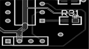
Understanding VCC, VEE, VDD, and VSS in Electronics
Meta Description Let us learn the differences between VCC, VEE, VDD, and VSS as used in electronics. We will review their definitions, circuit design roles, and practical applications in ICs, amplifiers, and microcontrollers. Introduction Modern electronic systems can not come to life if we put aside the power supply technology. The power supply is the backbone of every electronic circuit. Understanding the terminologies used in power supply forms the basis for designing functional projects. Terms like VCC, VEE, VDD, and VSS are standard in electronic datasheets, design documentation, and schematics, and designers and engineers should get all the concepts right. These are voltage naming conventions and essential in making it easy to understand power supply and pins available in electronic components such as ICs, amplifiers, and other operational circuits. This article gives a complete guide to these terms, their meaning, and their roles in a circuit. With such knowledge, you
How to Ensure PCB Quality Control Meets Industry Standards
Ensuring PCB quality control is essential for maintaining product reliability and meeting industry standards. Poor quality control often leads to defects, reduced performance, and costly product failures. Adhering to standards like IPC-6012 and ISO 9001 minimizes risks by enhancing durability and ensuring compliance. High-quality PCBs deliver optimal performance, reduce manufacturing costs, and build consumer trust. Robust testing and inspection processes, combined with strict adherence to these standards, create a foundation for consistent quality and long-term success. Key Takeaways Understanding PCB Quality Control Importance of PCB Quality Control PCB quality control plays a vital role in ensuring the reliability and functionality of electronic devices. Manufacturers aim to produce boards that are both dependable and fully operational. This process involves identifying and resolving potential issues early in production. By doing so, they reduce defects and improve the overall reliability of the manufacturing process. Effective quality control measures also enhance customer satisfaction by
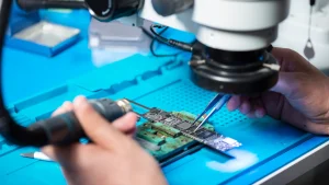
Understanding PCB Copy and Reverse Engineering Methods
Printed Circuit Board (PCB) copy and reverse engineering play a vital role in modern electronics. PCB copy involves replicating an existing board’s design to create identical functionality. Reverse engineering, on the other hand, dissects a PCB to understand its structure and operation. These methods are essential for solving challenges like replacing obsolete components or troubleshooting complex devices. For instance, engineers reverse engineered a critical PCB for a Florida power company, restoring operations after a shutdown. Globally, PCB reverse engineering has become a cornerstone of innovation, especially in regions like China, where it drives research and development. Key Takeaways What is PCB Copy and Reverse Engineering? PCB Copy: Definition and Purpose PCB copy involves duplicating an existing printed circuit board using technical methods. This process ensures the replicated board matches the original in functionality and design. You might use PCB copy to replace outdated components or create backups for critical systems.

How to Design Flexible PCB Stack-up for Optimal Performance
Designing a flexible PCB stack-up demands careful attention to material selection, layer configuration, and design challenges. You must balance performance, reliability, and cost-efficiency to achieve optimal results. Flexible PCBs offer unique advantages, such as reduced material usage and compact designs, which make them ideal for modern electronics. For instance, using simpler flex layer stacks with fewer copper layers can lower material and processing costs while maintaining flexibility. Additionally, efficient panelization reduces waste and enhances cost savings. Cost-Saving Strategies in Flexible PCB Design Strategy Benefit Efficient flex panelization Reduces overall manufacturing costs by optimizing panel surface area. By integrating connectors directly onto the substrate, you can further reduce material costs and simplify assembly. These considerations ensure your design remains both functional and economical. Key Takeaways Understanding Flexible PCB Stack-up What Is a Flexible PCB Stack-up? A flexible PCB stack-up refers to the arrangement of multiple layers in a flexible printed circuit
Why Rogers PCB Stands Out for High-Frequency Applications
When working with high-frequency applications, you need materials that deliver precision and reliability. Rogers PCB stands out because it offers superior signal integrity, ensuring clear and undistorted signals even at high speeds. Its low dielectric loss minimizes power dissipation, making it perfect for RF and microwave systems. You also benefit from improved thermal management, as Rogers materials dissipate heat effectively, protecting circuits from thermal damage. Additionally, these PCBs resist moisture and material degradation, making them durable in extreme environments. With these features, Rogers PCB ensures consistent performance in demanding applications. Key Point What is Rogers PCB? Rogers PCB is a high-performance circuit board material designed to meet the demands of advanced electronic systems. Unlike traditional PCBs, it uses specialized materials that deliver superior electrical and thermal properties, making it ideal for high-frequency applications. Material Composition Rogers PCB materials, such as the RO4000 and RO3000 series, stand out due to their

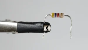
Resistor Color Code Guide for Beginners
Learning to decode a resistor color code might seem tricky at first, but it’s easier than you think. Start by identifying the bands from the edge closest to the first stripe. Watch out for common pitfalls like confusing similar colors or reading the bands backward. Good lighting and practice make all the difference! Key Takeaways Basic Principles of the Resistor Color Code What is a Resistor? A resistor is a tiny but important part of electronics. It slows down the flow of electricity in a circuit. This slowing is called resistance, measured in ohms (Ω). The unit is named after Georg Ohm, a German scientist. Bigger values are written as kilo-ohms (kΩ) or mega-ohms (MΩ). For example, 1 kΩ equals 1,000 ohms, and 1 MΩ equals 1,000,000 ohms. Why is resistance important? It controls how much electricity moves in a circuit. If you double the voltage, the current also doubles.
What is a 10k Resistor and How It Works
What is a 10k Resistor? A 10k resistor is an electronic component with a resistance value of 10,000 ohms. It limits the flow of electrical current in a circuit, ensuring components operate safely and efficiently. The “10k” refers to its resistance value, measured in ohms (Ω), which is a standard unit in electronics. Resistors like this play a crucial role in controlling current and voltage, making them essential in both simple and complex circuits. The Role of Resistors in Electronic Circuits Resistors are the backbone of electronic circuits. They regulate current, divide voltage, and protect sensitive components from damage. For example, a resistor can limit the current flowing to an LED, preventing it from burning out. Resistors also help create timing circuits, filter unwanted frequencies, and match the impedance between different parts of a circuit. Without resistors, circuits would lack stability and precision. The 10k resistor, in particular, is a

Wonderful PCB Holds Annual Meeting: Reflecting on Achievements and Setting New Goals for the Future
Wonderful PCB, a leading manufacturer of PCBs and flexible PCBs, recently held its much-anticipated annual meeting, bringing together the company’s leadership, employees, and stakeholders. The event was an opportunity to reflect on the company’s achievements over the past year, acknowledge the hard work of the team, and set ambitious goals for the year ahead. Celebrating Successes The meeting began with a review of the company’s key accomplishments, including notable growth in production capacity, successful collaborations with global clients, and the expansion of services in flexible PCB manufacturing and assembly. Wonderful PCB has become a trusted partner for companies worldwide, delivering high-quality products and innovative solutions in electronic manufacturing. Recognizing Outstanding Contributions During the meeting, the company also recognized several employees for their outstanding contributions. Special awards were given to individuals who have shown exceptional leadership, dedication, and teamwork throughout the year. These recognitions highlight the importance of each team member
A Comprehensive Guide to Electronics Design Services and the Design Process
1. What Are Electronics Design Services, and What Is the Electronics Design Services Process? Electronics design services refer to the designing, testing, and manufacturing of electronic products such as IoT devices, industrial controls, and medical equipment. This process involves transforming ideas and concepts into market-ready products, which requires expertise in electrical engineering, mechanical design, and software development. These services span the entire development cycle—from early concept ideation to the final product in the market. The electronics design process typically includes the following stages: 2. The Electronics Design Process The electronics design process typically includes the following stages: 3. Why Outsource Electronic Design Projects? Outsourcing electronic design projects offers several benefits: 4. Electronics Product Design Key Stages The typical key stages in the electronics product design process include: 5. How to Select an Electronics Design Engineer When selecting an electronics design engineer, consider the following factors: 6. Electronics Product Design and

Chinese New Year holiday 2025
Please be informed that Wonderful PCB will be closed for the Chinese New Year holiday from January 23 to February 4. During this period, our office and production facilities will be temporarily unavailable. We apologize for any inconvenience this may cause and appreciate your understanding. Our team will respond to any inquiries and resume regular operations after February 4. Thank you for your continued support, and we wish you a prosperous and joyful New Year! Best regards,The Wonderful PCB Team

The Importance of Mark Points in PCB Design for SMT
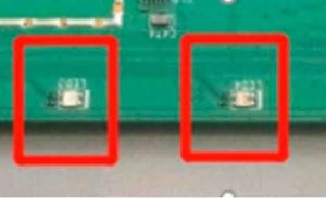
Mark points, also known as optical marks or reference points, are critical for component assembly in PCBs, particularly in the context of PCBA (Printed Circuit Board Assembly) for automatic placement machines. The choice and placement of Mark points directly impact the efficiency of the automatic pick-and-place machine, so it’s essential to carefully design these points and their positions within the board. Mark Point Design Single-Sided PCB Mark Points When designing a PCB, Mark points should be added on the side that will be populated by components. For double-sided assembly, Mark points should be added on both sides. Typically, Mark points are placed at the four corners of the PCB, ensuring the positions are asymmetrical to prevent incorrect usage. If space is limited, at least three Mark points should be added, and if the design is very tight, at least two Mark points should be placed diagonally across from each other.
The Importance of Component Layout Near PCB Edges in PCBA
The proper placement of electronic components on a PCB (Printed Circuit Board) is a critical factor in reducing soldering defects. A well-planned layout plays a significant role in the overall quality of the assembly. When designing the layout, components should be placed in areas with minimal bending and internal stress, and their distribution should be as uniform as possible. This is especially important for components with high thermal conductivity, where large PCBs should be avoided to minimize expansion and contraction. Poor layout design can adversely affect both the tradeability and stability of the PCB. In many cases, designers, in an effort to maximize the use of available space, may place components as close as possible to the board’s edges. This practice, however, can present significant challenges in manufacturing and PCBA assembly. In some cases, it can even lead to problems during soldering or assembly. The Risks of Placing Components Near
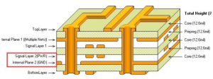
PCB stack-up Planning and Configuration
One of the most fundamental considerations in PCB design is determining how many routing layers, ground planes, and power planes are needed to meet the circuit’s functional requirements. The stack-up design of the PCB is usually a compromise, taking various factors into account. Below are the key principles for PCB stack-up design. stack-up Planning Outer Layers with GND and PWR: These layers are primarily used for routing and shorting out traces. For HDI (High-Density Interconnect) applications, the second layer is often a signal layer used for routing traces between fine-pitch BGA components. In this HDI application, manufacturers typically use laser drilling for controlled-depth drilling to access the second layer. Balancing Layers: All stack-ups must have a balanced layer stack-up from the PCB’s central line to minimize or eliminate warping. The type and thickness of the prepreg (pre-impregnated material) must be determined before starting the CAD layout. Manufacturing Considerations: It is
PCB Shape Nesting Examples for PCB Assembly
For PCB nesting, engineers are familiar with the basic rules, such as spaced or non-spaced nesting, using V-CUT or stamp holes for connections, adding process edges, positioning holes, and mark points. However, PCB come in various shapes, and simply following these basic rules is not enough. It is crucial to understand the production process in detail to ensure proper nesting, which will help avoid issues that may render the PCB unproducible or result in production scrap. The following examples highlight different PCB shape nesting cases for educational purposes. CNC + V-CUT Nesting Using Milling + V-CUT Nesting Method: In this case, the nesting is done without spacing on the top, bottom, left, and right edges. If the PCB’s outer shape has irregular notches, non-spaced nesting becomes impractical. This is because small notches, which are smaller than the milling tool’s radius, cannot be milled properly, and burrs might form after milling.

PCB Pad Design Issues Explained
The assembly quality of SMT (Surface Mount Technology) is directly related to the PCB pad design, and the size ratio of the pads is crucial. If the PCB pad design is correct, minor misalignment during placement can be corrected during the reflow soldering process (known as self-alignment or self-correction effect). On the other hand, if the PCB pad design is incorrect, even precise placement can result in component misalignment, solder bridges, and other soldering defects after reflow soldering. Basic Principles of PCB Pad Design Based on the analysis of various component solder joint structures, to ensure the reliability of the solder joints, the PCB pad design should focus on the following key factors: Solderability Defects Caused by Pad Size Inconsistent Pad Sizes Pad sizes must be consistent, and their length should be within an appropriate range. Pads that are too short or too long can cause the “tombstoning” (standing up)

How to Avoid Pitfalls in PCB Hole and Slot Design
In the design of electronic products, from creating the schematic to PCB layout and routing, various errors can occur due to a lack of experience or knowledge, which can hinder progress and, in severe cases, render the circuit board unusable. To prevent such issues, it is essential to improve our understanding of this area and avoid common mistakes. This article will discuss some common drilling issues during PCB design to help you avoid repeating the same mistakes. Drilling can be categorized into three types: through-hole, blind hole, and buried hole. Through-holes include plated through holes (PTH), non-plated through holes (NPTH), and vias, all of which serve to provide electrical connectivity between layers. Regardless of the type, missing holes can lead to significant functional failures, making correct drilling design crucial. Problem 1: Slot Holes Placed on the Wrong Layer in Altium Design Problem 2: Zero-Diameter Holes in Altium Design Problem 3:
Do You Understand the Four Major PCB Testing Methods?
A PCB (Printed Circuit Board) is an essential electronic component, often referred to as a printed circuit or printed wiring board. The quality of the PCB largely determines the performance of electronic components, making testing a critical part of the PCB production process. Testing typically identifies functional defects, such as opens, shorts, and other issues that are not easily visible. To ensure the success of any product design, multiple rounds of testing are necessary. PCB testing helps minimize major issues, identify smaller errors, save time, and reduce overall costs. PCB testing is mainly used to address potential problems during the manufacturing and final production stages. These tests can also be applied to prototypes or small-scale assemblies to identify potential issues with the final product. Testing Methods for Bare PCB 1. AOI Testing (Automatic Optical Inspection) AOI equipment is widely used across various industries, including PCB manufacturing, as a key quality assurance
8 Safety Distances That Must Be Considered in PCB Design
There are many safety distance considerations in PCB design, including spacing between traces, character spacing, pad spacing, and more. Here, we classify them into two categories: electrical-related safety distances and non-electrical-related safety distances. 01 Electrical-Related Safety Distances Trace-to-Trace Spacing For the processing capabilities of mainstream PCB manufacturers, the minimum distance between traces should not be less than 0.075mm. The minimum trace spacing refers to the smallest distance between a trace and another trace or between a trace and a pad. From a manufacturing perspective, larger trace spacing is better. A more common value is 0.127mm. Pad Hole Diameter and Pad Width For mainstream PCB manufacturers, if the pad uses mechanical drilling, the minimum hole diameter should not be less than 0.2mm. If laser drilling is used, the minimum hole diameter should not be less than 0.1mm. The hole diameter tolerance may vary slightly depending on the material, but it is