Many engineers get confused when they compare pwb vs pcb. The main difference is in what each one does and what people call them. A printed wiring board (PWB) only has the wiring pattern. A printed circuit board (PCB) has both wiring and parts attached. In 2025, the pwb vs pcb debate still affects design choices, quality checks, and how boards are made. Knowing this difference helps teams pick the right board for their project needs.
Key Takeaways
PWBs have only wiring patterns. PCBs have wiring and electronic parts. PCBs make a full circuit.
You pick PWB or PCB based on your project. Think about how hard the project is, how much it costs, and what it needs to do. PWBs are good for simple and cheap designs. PCBs are better for hard and fast devices.
Both PWBs and PCBs use materials like FR-4 and polyimide. But PCBs often need better materials. These help with heat and let them have more layers.
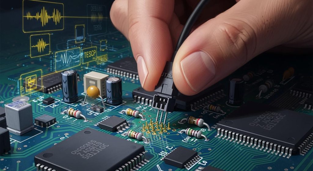
Today, factories use machines and smart tools to make PWBs and PCBs. This makes them faster and better. PCBs need even more advanced steps.
Knowing the difference between PWBs and PCBs helps engineers choose the right board. It saves money and helps them build strong electronics for today’s world.
PWB vs PCB Overview
Printed Wiring Board
A printed wiring board, or PWB, is the base for most electronics today. The PWB is a flat board that does not conduct electricity. It has special lines called traces that carry signals. These traces connect different spots on the board. Long ago, engineers used wires to connect parts. This made things big and hard to fix. The printed wiring board made things easier.
Printed wiring boards started in the early 1900s. In 1903, Albert Hanson had an idea using metal strips and holes. In 1925, Charles Ducas put circuit shapes on special boards. He helped start the idea of printed circuits. Paul Eisler made a big change in 1936. He used foil and made radios with the first real PWB. During World War II, the U.S. military used these boards in bombs. This showed how important they were.
Note: “Printed wiring board” means a board with only the wiring pattern. It does not have any parts on it. This helped engineers plan the board before adding anything else.
The table below shows important events in printed wiring board history:
Year/Period | Milestone/Event | Description/Significance |
|---|---|---|
1831 | Faraday’s Law of Electromagnetic Induction | This law helped people understand how electronics work. |
1887 | Hertz confirms Maxwell’s prediction of electromagnetic waves | This made people excited about radio and new tech. |
1903 | Albert Hanson applies for a British patent | He had an early idea for making boards with metal strips and holes. |
1907 | Leo Hendrik Baekeland industrializes phenolic resin production | He made a new material that helped make better boards. |
1925 | Charles Ducas prints circuit patterns on insulating substrate | He used a new way to make wiring and called it “PCB.” |
1936 | Paul Eisler publishes foil technology and applies PCB in radios | He made boards by removing extra metal, like we do today. |
1942-1943 | Paul Eisler invents and patents the first practical double-sided PCB | He made boards with wiring on both sides, which was a big step. |
1943 | US military uses PCBs for proximity fuzes in WWII | The military used these boards in war for the first time. |
1947 | Epoxy resin introduced for PCB substrates | New materials made boards stronger and better. |
1948 | US officially recognizes PCBs for commercial use | People could now use PCBs in things other than the military. |
1950s | Transistors replace electron tubes; etching becomes dominant PCB manufacturing method | New parts and ways to make boards helped them spread everywhere. |
1953 | Motorola develops double-sided boards with electroplated vias | This helped make boards with more layers. |
1960s | Multilayer PCBs begin mass production; plated through-hole technology matures | Boards got more layers and could do more things. |
1958 | Invention of integrated circuits by Robert Noyce and Kilby | Tiny circuits made boards even more important. |
1971 | Intel launches first microprocessor (4004) and 1kb DRAM | New chips made boards more complex and useful. |
1980s | Surface mount technology (SMT) replaces through-hole mounting; CAD software emerges | Boards became faster to design and build. |
1993 | Paul T. Lin patents BGA packaging | New ways to package parts made boards better. |
1995 | Panasonic develops BUM PCB manufacturing technology | Boards could now fit more parts in small spaces. |
Early 2000s | PCBs become smaller, more complex; flexible PCBs become common | Boards got smaller and could bend for new devices. |
2006 | Development of Every Layer Interconnect (ELIC) process | Boards could now connect layers in new ways. |
2010s | ELIC PCB technology gains wider adoption | Phones and new gadgets used these advanced boards. |

Printed Circuit Board
A printed circuit board, or PCB, starts with a PWB. The PCB has the wiring pattern and also has parts on it. These parts are things like resistors, chips, and connectors. The PCB holds these parts and connects them. This makes a full working circuit.
People started saying “printed circuit board” after Paul Eisler’s work in 1936. By the 1940s, the U.S. military used PCBs in weapons. In 1948, the U.S. government said PCBs could be used in business. This made the electronics world grow fast. PCBs changed from simple boards to ones with many layers. Each layer has tiny paths for electricity. This lets devices be smaller and stronger.
PCBs have changed a lot over time:
In the 1960s, calculators used PCBs with about 30 transistors. Now, computers have millions of transistors on one chip.
Parts like capacitors and resistors are much smaller now.
The first home computers in the 1970s used more complex PCBs.
The PCB market was worth over $85 billion in 2022. It may be more than $100 billion by 2026. The chip carrier part grew by 40% in just one year.
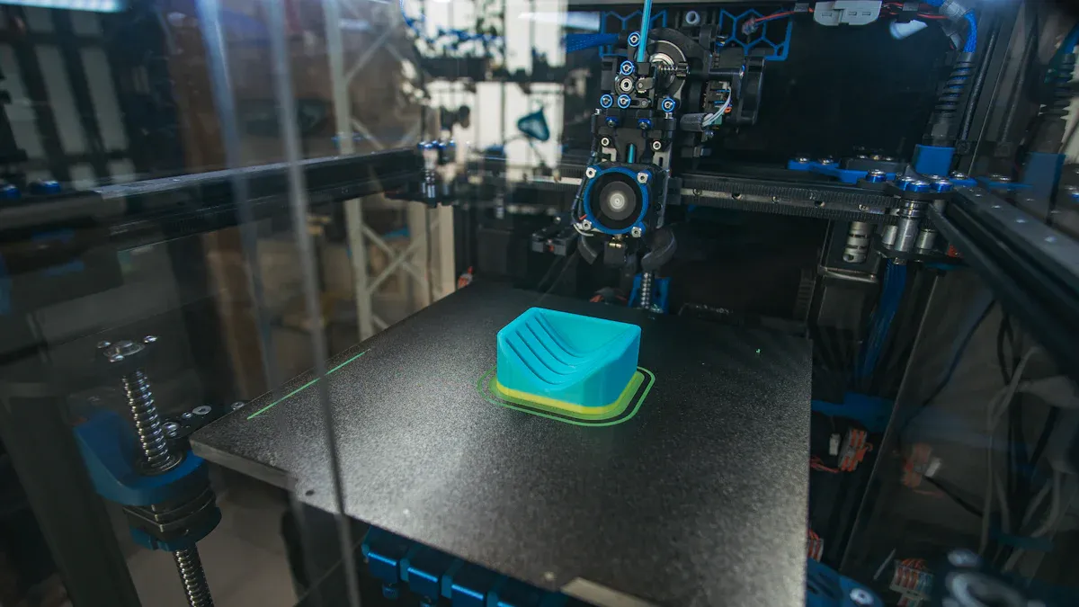
The PCB industry grew fast because of new materials, 3D printing, and tiny connections. These changes help make smaller and stronger devices.
How the Terms Have Evolved
The words PWB and PCB have changed over time. Long ago, “printed wiring board” meant a board with just the wiring. When parts were added, it was called a “printed circuit board.” As technology got better, people stopped making a big difference between the two. Now, most people use both words to mean the same thing, unless they work in special jobs.
Switching from hand-wired boards to printed circuits was a big deal. Old devices used wires that were slow and broke easily. Printed circuits made things faster, stronger, and easier to fix. PCBs have layers of metal and non-metal. These layers hold parts and connect them. This makes a full circuit.
In short, the pwb vs pcb talk shows how things have changed. The story of printed wiring boards shows how we went from simple boards to very complex ones. Today, picking a PWB or PCB depends on how many parts you need and what you want the board to do.
Materials and Structure

PWB Materials
Engineers pick pwb materials based on what the circuit needs. They also think about where the board will be used. The substrate is the main part of every pwb. Most pwbs use fiberglass-reinforced epoxy like FR-4 as the base. Some boards need polyimide or ceramic substrates for better heat control. The wiring pattern is made from a copper layer. What the pwb is made of changes how well it handles heat, keeps electricity inside, and stays strong.
A comparison of pwb laminate materials shows how choices affect how the board works. The table below lists important properties:
Laminate Material | Usage Scope | Performance Description | Glass Transition Temperature (Tg, °C) | Electrical RTI |
|---|---|---|---|---|
Laminate A | Widely Used | Standard Performance Epoxy | 180 | 130 |
Laminate B | Limited Use – Application Specific | High Speed Performance – Non-Epoxy Filled | 200 | 130 |
Laminate C | Limited Use – Application Specific | High Temperature Resistant – Filled | 190 | 130 |
Laminate D | Limited Use – Application Specific | High Temperature Resistant – Filled | 160 | 160 |
Laminate E | Specific Use (RF) | High Temperature / Microwave – Filled | >280 | 160 |
Keeping the pwb cool is very important for it to work well. Tests like UL746A and IEEE STD 98 help check how long a pwb lasts when it gets hot. Picking the right materials helps the board handle high heat and keep working. Engineers also test if the board can stop electricity from leaking and if it stays strong over time.
PCB Materials
A pcb starts with a pwb but has more parts and layers. The pcb substrate often uses the same materials as a pwb, like FR-4. Some advanced pcbs need special laminates or metal-core substrates to handle more heat. A pcb is made of the substrate, copper traces, solder masks, silkscreen layers, and sometimes extra built-in parts.
As circuits get smaller and closer together, keeping the pcb cool gets harder. The materials used help the pcb move heat away from busy parts. Some high-end pcbs use ceramic or aluminum substrates to help with heat. Making a pcb means matching the materials so they stick together, can be shaped right, and parts can be attached well.
Engineers look at how each material handles heat, stops electricity from leaking, and stays tough. The best mix of materials helps the pcb last longer and work with hard circuits. What materials are picked changes how the pcb is made, how much it costs, and what it can do. In 2025, designers keep looking for better materials that help with heat and support new, advanced circuits.
Manufacturing Process
PWB Production
Making a pwb starts with picking the right base. Most pwbs use phenolic paper or epoxy glass. The first step is to make the wiring pattern. This is done with photolithography or screen printing. Next, chemical etching takes away extra copper. Only the needed traces stay on the board. This makes the base for the circuit card assembly.
Long ago, people made pwbs by hand. They placed and etched patterns themselves. Now, machines do most of the work. Automation makes things faster and helps avoid mistakes. Takt time shows how fast a unit is made. Changeover time tells how quickly the line switches products. Defect density counts bad units in a batch. First pass yield shows how many units are right the first time. The table below lists important production numbers:
Metric | What it Measures | How it Quantifies Efficiency Gains in PWB Production |
|---|---|---|
Takt Time | Time to produce a unit to meet customer demand | Indicates production speed and balance with demand, avoiding over/underproduction |
Changeover Time | Time to switch production between products | Reduces downtime and idle machines, improving output |
Defect Density | Number of defective units per batch | Identifies quality issues early, reducing waste and rework |
First Pass Yield (FPY) | Percentage of units produced correctly first time | Reflects process efficiency and quality, minimizing rework |
Overall Equipment Effectiveness (OEE) | Combines availability, performance, and quality | Identifies equipment-related inefficiencies and waste |
Modern pwb factories use less power and make fewer mistakes. AI and robots help boost output by over 26%. These tools help companies learn and improve faster. This means pwbs now handle heat better and last longer.
PCB Production
Making a pcb starts with a strong base like FR-4 or polyimide. The process uses new tools like laser direct imaging and inkjet printing. Multilayer lamination lets boards have more complex circuits. These steps help manage heat better.
Most pcb factories use automated lines. Pick-and-place machines put on up to 40,000 parts each hour. This is much faster than people can do by hand. Automation lowers mistakes and cuts labor costs by up to 30%. IoT helps with predictive maintenance and cuts downtime by 70%. Big companies use robots and real-time checks to keep quality high and waste low.
The table below shows how pwb and pcb production compare:
Aspect | PWB Production Characteristics | PCB Production Characteristics |
|---|---|---|
Manufacturing | Simpler processes: photolithography, screen printing, chemical etching | Advanced techniques: laser direct imaging, inkjet printing, multilayer lamination, complex drilling/plating |
Materials | Lower-cost substrates: phenolic paper, epoxy glass | Higher-performance substrates: FR-4, polyimide, Rogers materials |
Cost | Lower material and manufacturing costs; suitable for low-volume, simple designs | Higher costs due to advanced materials and processes; benefits from economies of scale in high-volume production |
Design Complexity | Suitable for single-sided, less complex boards | Supports multilayer, high-density, complex circuit designs |
Performance & Reliability | Basic signal integrity, thermal management, mechanical stability | Superior signal integrity, thermal management, mechanical stability, environmental resistance |
Industry 4.0 tools now help make pcbs. Automated optical inspection finds defects very well. Additive manufacturing lets companies make quick samples. Design for manufacturing tools help plan the assembly process. These new ideas help make better printed wiring assemblies and increase output. Now, pcb factories make boards that handle heat better and work for modern electronics.
Applications
Choosing PWB
Engineers pick a pwb when they need a simple design. PWBs are good for school kits, basic gadgets, and easy home devices. These boards are best for circuits that are not complicated. Cost and speed are the most important things for these uses. PWBs cost less to make and are fast to build. This makes them great for projects with small budgets. Their paths for electricity do not change, so they are not very flexible. But they still work well for easy jobs.
The table below shows what to think about when picking a pwb or pcb:
Decision Factor | PWBs | PCBs |
|---|---|---|
Complexity | Simpler design | Supports complex, multi-layer circuits |
Cost | Lower manufacturing costs | Higher cost, justified by performance |
Production Volume & Time | Faster turnaround, ideal for low volume | Suitable for large-scale production |
Application Examples | Educational kits, simple appliances | Telecommunications, advanced computing |
Performance | Limited for high-speed applications | Enhanced signal integrity |
Design Flexibility | Less adaptable | Highly customizable |
Testing & QA | Suitable for simpler boards | Advanced testing methods |
Tip: Think about how hard your project is and how much money you have. PWBs are best for quick tests and learning.
Choosing PCB
A pcb is used for hard jobs that need to work really well. PCBs can have many layers and lots of parts close together. This is needed for phones, computers, and tiny devices. These boards keep signals clear and block unwanted noise. That is why people use them for tough jobs.
PCBs use special tests like looking with machines, X-rays, and checking circuits. These tests help make sure the boards are good and safe to use. A report says the board market will be worth $15.8 billion by 2032. This is because more people need boards for schools, businesses, and governments, especially in Asia Pacific.
Engineers pick a pcb when they need something strong, flexible, and able to do a lot. PCBs can fit tricky designs and work with new digital tech.
PWB and PCB are made from similar stuff and started the same way. But they are not the same in how hard they are to make, how they are put together, and how well they work. The table below shows how they are different:
Aspect | PWB | PCB |
|---|---|---|
Function | Carrier for manual wiring | Complete board with embedded components |
Design Flexibility | High, allows rewiring | Low, permanent design |
Reliability | Lower due to manual connections | Higher with automated assembly |
Picking the best board in 2025 depends on what your project needs. You also need to think about rules and what you might use the board for later. Companies should:
Pick a board that fits their type of work, how much risk they can take, and their tech plans.
Keep an eye on new rules and ways to help the planet.
Use both people and AI together to make smarter choices.
Boards that are just right for today’s tough jobs will help companies do well.
FAQ
What is the main difference between a PWB and a PCB?
A PWB only has the wiring pattern. A PCB has both the wiring and the electronic parts attached. Engineers use PWBs for planning and PCBs for finished products.
Can engineers use PWB and PCB for the same project?
Yes, they can. Teams often start with a PWB to design the wiring. They use a PCB when they add all the parts and finish the device.
Why do some companies still use the term PWB in 2025?
Some industries, like aerospace and defense, use “PWB” for boards without parts. This helps them follow strict rules and avoid confusion during inspections.
Are the materials for PWBs and PCBs the same?
Most PWBs and PCBs use similar base materials, such as FR-4 or polyimide. The main difference comes when engineers add parts and extra layers to make a PCB.
How does the choice between PWB and PCB affect cost?
PWBs usually cost less because they are simpler. PCBs cost more due to extra parts, layers, and testing. The right choice depends on the project’s needs and budget.