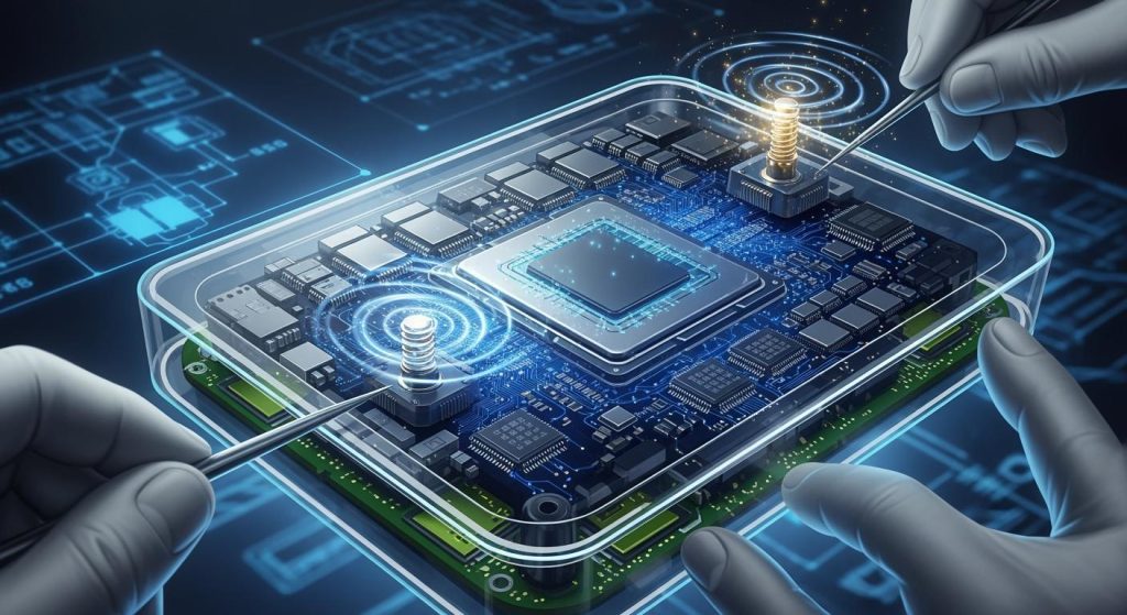
You see new changes in mobile PCB design for smartphones that reflect the latest trends. These changes help make phones work better and get made faster. Now, there is a big push to make things smaller. Designers use high-density interconnects and multi-layer PCBs. These new ideas let you have thinner and stronger smartphones. Your phone can now use cool features like 5G and AI.
The mobile PCB market grows quickly, driven by the latest trends as people want smaller, faster, and better devices.
You want smartphones that do more and connect faster, aligning with the latest trends in technology.
New uses like augmented reality help these trends grow.
Impact Area | Description |
|---|---|
Miniaturization | Lets you have slimmer phones without losing battery or features, in line with the latest trends. |
Embedded Components | Uses fewer parts, so makers save up to 20% of production time, reflecting the latest trends in efficiency. |
Advanced Materials | Helps phones support 5G, AI, and be better for the environment, showcasing the latest trends in sustainability. |
Learning about new PCB design trends helps you see how the latest trends are changing future smartphones.
Key Takeaways
Miniaturization in PCB design helps phones get thinner and lighter. Phones still work well with this change.
Multi-layer PCBs fit more parts into small spaces. This makes phones work better and last longer.
Embedded components make devices smaller and work better. Devices also become more powerful.
Flexible and 3D PCBs help create new phone designs. Phones can fold and last longer with these PCBs.
Eco-friendly materials in PCB making help the planet. These materials also make devices work better.
Latest Trends in PCB Design
Miniaturization & HDI PCBs
Miniaturization is changing mobile phone pcbs. New smartphones are thin and light. This happens because pcb design is getting better. High-density interconnect, or hdi, technology helps a lot. HDI lets more connections fit in small spaces. Phones have more features but do not get bigger.
Here is a table that shows new miniaturization and hdi pcb technology:
Advancement Type | Description |
|---|---|
High-Density Interconnect | Lets more connections fit in small spaces, great for small devices. |
Flexible PCBs | Helps make devices smaller and allows cool new shapes. |
Advanced Materials | Makes pcbs work better and last longer in phones. |
Makes designing faster and easier. | |
3D Printing | Changes how things are made, helps create new designs fast. |
HDI pcbs let parts sit close together. Phones can have more cameras and better processors. HDI uses microvias and fine traces to stack layers. This makes the printed circuit board smaller. It also helps signals move better. Phones get faster data and work more efficiently. Miniaturization in pcb design gives you advanced features in a small device.
Multi-Layer PCB Adoption
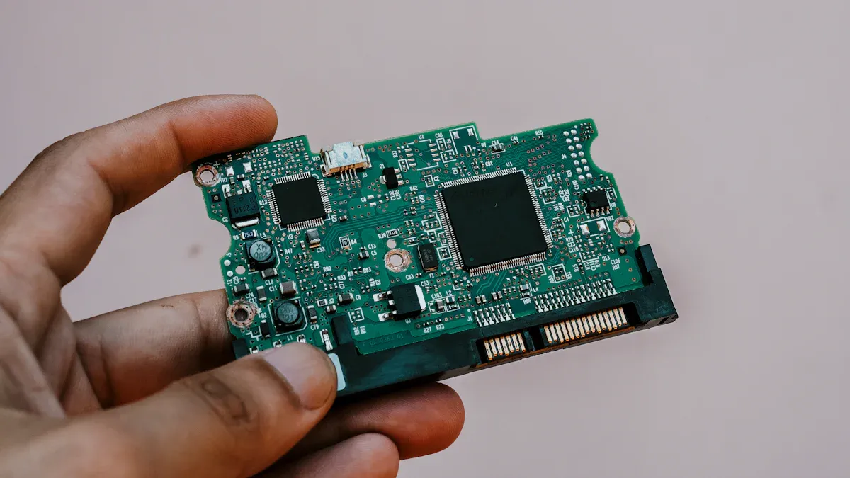
Smartphones have lots of power in small spaces. Multi-layer pcbs make this possible. Most new phones use multi-layer pcb board layout design. These pcbs have many layers stacked up. This lets them hold more parts and complex circuits.
Compact Size: Multi-layer pcbs fit complex designs in small spaces.
Lightweight Design: They use fewer big parts, so phones are lighter.
High Reliability and Durability: Inside connections are strong and last longer.
High Component Density: More parts fit in small areas, so phones do more.
Support for Complex Circuits: Extra layers help with tricky designs.
Enhanced Performance: Good design means signals move faster and better.
Multi-layer pcbs help power move well and keep signals clear. Phones get steady voltage and less noise. This means your phone works better and lasts longer. Here is a table that explains the benefits:
Benefit | Explanation |
|---|---|
Improved Power Distribution | Multi-layer pcbs spread power well, so voltage stays steady. |
Increased Functionality | They have room for complex circuits, needed for modern phones. |
Improved Signal Integrity | Multi-layer designs cut down on interference, good for fast phones. |
Enhanced Reliability | Extra protection keeps devices working longer. |
Multi-layer pcb board layout design makes phones smaller, stronger, and more efficient. This trend helps phones meet the need for speed and lots of features.
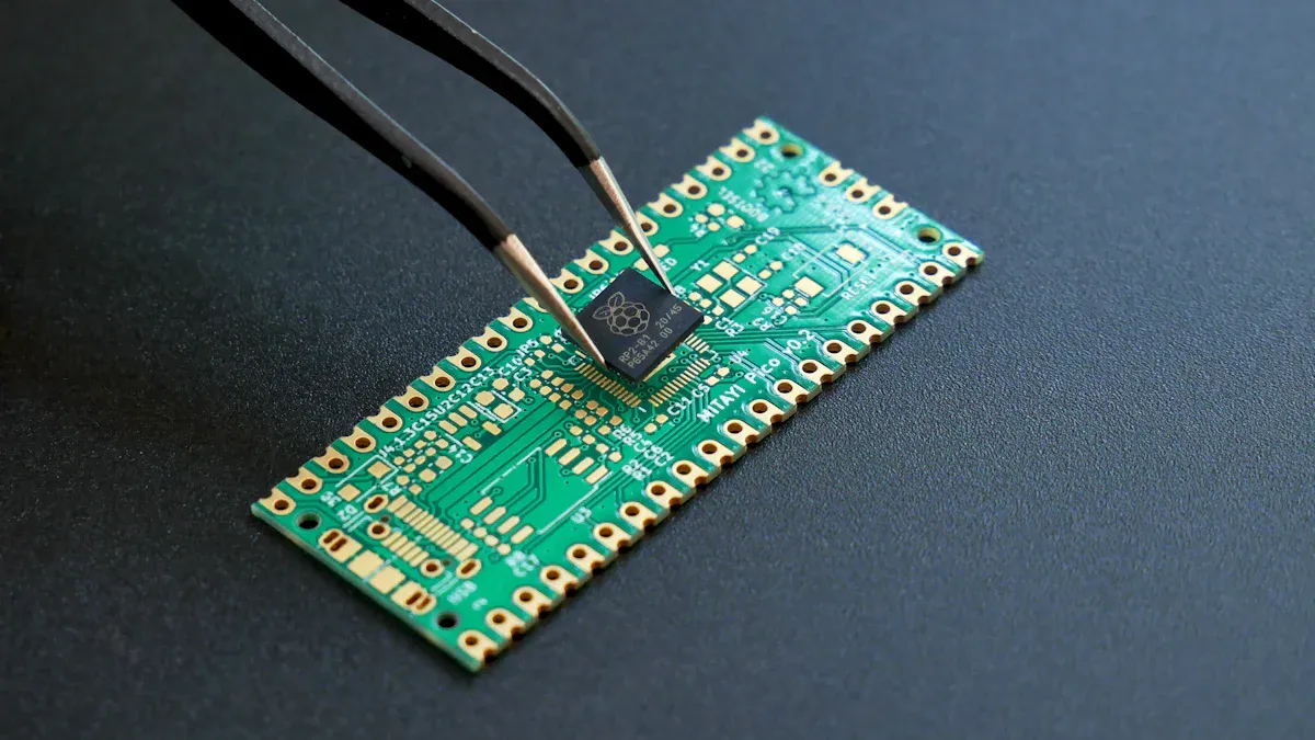
Embedded Components Integration
Mobile phone pcbs are changing with embedded components. Makers put parts right into the pcb substrate. This saves space and makes phones thinner. You get phones that are light and powerful.
Embedded components go inside the pcb substrate, saving space.
This helps performance by lowering unwanted effects and making signals better, important for things like 5G.
Makers can get impedance as low as 25 ohms, which helps data move fast.
Fewer solder joints mean lower costs and better reliability.
Miniaturization methods like System-in-Package (SiP) add more features to small devices.
Putting passive parts inside and using SiP is more common now.
These ways shrink the size and make electrical performance better.
Using embedded components in mobile phone pcbs gives you many benefits:
More pcb density: Putting passive parts inside can shrink pcb size by about 25%, so phones are smaller.
Better pcb assembly reliability: Fewer solder points mean fewer problems, so phones last longer.
Better electrical performance: Embedded parts lower unwanted effects, so phones use power better and stay stable.
Smartphones get thinner, lighter, and stronger with embedded components in printed circuit boards. This way of designing pcbs gives you sleek and high-performing phones. You see how new pcb board layout design and embedded components make modern mobile phone pcbs work better.
Tip: Learning about these pcb design trends helps you know why your smartphone is efficient, reliable, and full of features. Knowing these trends helps you pick better devices.
Flexible & 3D Mobile Phone PCBs
Flexible PCB Applications
Many smartphones use flexible and stretchable pcbs now. These pcbs help make phones thin and light. You can also find them in tablets, cameras, and wearables. Flexible and stretchable pcbs connect parts without big cables or connectors. This makes your device smaller and easier to carry. Foldable phones use flexible and rigid-flex pcbs so they can bend and fold. You can open and close your phone many times, and it still works well. High-speed data keeps moving fast in these designs.
Flexible and stretchable pcbs let phones have new shapes and styles.
They make devices stronger and help stop broken connections.
Devices can be smaller and have more cool features.
3D PCB Structures
Smartphones use 3D PCB structures to save space and add more features. Flexible and rigid-flex pcbs mix stiff and bendy layers together. This lets designers put more parts in small spaces. Rigid-flex pcbs help make phones thin and light. Signals travel shorter paths, so phones work faster and better. System-in-Package technology puts many modules in one place. This makes your phone smarter and quicker. Embedded parts inside the pcb help make phones smaller and work smoothly.
Feature | Benefit for You |
|---|---|
Higher Component Density | More features in a smaller phone |
3D Configuration | Thinner and lighter devices |
Shorter Routing Paths | Faster data and better performance |
Durability & Manufacturing Benefits
Flexible and stretchable pcbs make your phone strong and reliable. These pcbs can bend, twist, and take hits without losing power. You can use your phone in tough places, and it will still work. Flexible and rigid-flex pcbs need fewer extra connectors, so there are fewer things that can break. This helps your device last longer. Makers like these pcbs because they are easier to put together and weigh less. Rigid-flex pcbs also help keep signals clear and stop interference, which is good for fast phones.
Tip: Flexible and stretchable pcbs help you get phones that are strong, light, and full of features. You get devices that look cool and work well, even after lots of use.
Advanced & Sustainable Materials
High-Frequency and Low-Loss Materials
New materials in mobile phone PCBs help your phone work better. These materials keep signals strong and clear. This is important for 5G and fast data. Rogers and PTFE PCBs are used a lot. They have low loss and stay stable. Your phone can handle high frequencies with these materials.
Material | Key Features | Applications in Mobile Phones |
|---|---|---|
Rogers PCB | Low dielectric loss, stable constant, thermal stability | Used in antennas, power amplifiers, filters |
PTFE PCB | Ultra-low loss, low constant, high thermal and chemical resistance | Used in RF circuits, base station parts, antennas |
These materials help stop signal loss. They keep data moving fast. Low-loss materials also cut down on noise. Your phone works smoothly with them. You need these features for new things like 5G.
High-frequency and low-loss materials keep your data safe and fast.
They help your phone avoid noise and keep signals strong.
You get better performance and more reliable connections.
Thermal Management Solutions
Phones get hot when you play games or watch videos. Makers use smart ways to control heat in PCBs. They use tools to check how heat moves and change designs. Thicker boards spread heat better. Metal-core PCBs move heat away from hot parts. Good airflow can lower the temperature by up to 10°C. Testing with thermal imaging finds hot spots and helps fix problems.
Use tools to model heat and change designs.
Make boards thicker to spread heat better.
Pick metal-core PCBs for good heat movement.
Improve airflow to keep your phone cool.
Use thermal imaging to check real-world heat.
Advanced thermal management helps your phone last longer. These solutions move heat away from important parts. Your device stays reliable and works well.
Tip: Good thermal management means your phone works well and does not break from overheating.
Eco-Friendly PCB Materials
You care about the planet, and so do phone makers. They use eco-friendly substrates and biodegradable materials. Cellulose-based composites are one example. These choices help the environment and cut down on waste. More companies use bio-based substrates and green chemistry. This lowers toxicity and energy use. Rules like the EU’s RoHS and REACH push makers to use safer materials.
Eco-friendly PCB materials cut down on hazardous substances.
Bio-based substrates and green chemistry lower energy use.
Government rules encourage low-carbon, recyclable PCBs.
Sustainable practices help protect the planet and drive innovation.
You help the planet when you pick devices with eco-friendly PCBs. These materials make smartphone manufacturing safer and greener.
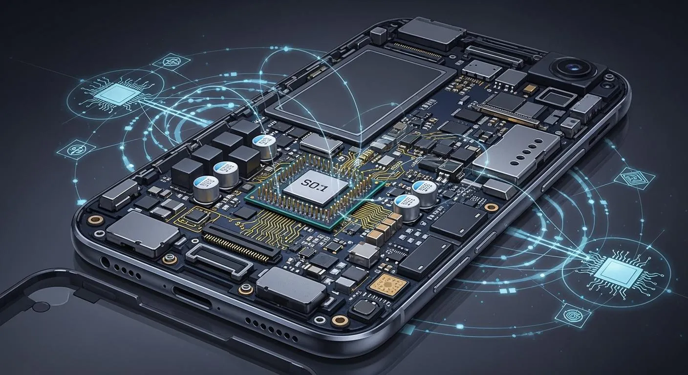
5G and AI in Mobile Phone PCB Market
The mobile phone pcb market is changing quickly because of 5G and AI. New designs help your phone work faster and better. These changes make high-performance smartphones possible. They also let phones have more advanced features.
5G PCB Design Requirements
Phones need special pcb designs to use 5G. These designs help your phone handle fast signals and lots of data. To do this, you must:
Match impedance, usually 50 ohms, to stop signals from bouncing back.
Keep trace lengths short so signals do not get weak.
Use ground planes for high-frequency signals and less EMI.
Use fewer vias to lower inductance and capacitance.
Pick low-loss materials and shield traces to stop crosstalk.
Make trace lengths the same for differential pairs to control timing.
Use simulation tools to check signals before making the pcb.
Thermal management is important too. You need heat sinks, thermal vias, and good placement of hot parts. Antenna design matters a lot. 5G uses phased array antennas and beamforming. These must fit in small spaces. The mobile phone pcb market now needs these advanced designs to keep up with new technology.
Evidence Point | Explanation |
|---|---|
Global 5G Network Expansion | More 5G means more need for advanced pcbs. |
Increasing Data Consumption | Streaming and gaming need efficient pcbs. |
Technological Advancements in Devices | New features require complex, high-performance pcbs. |
Growth in IoT and Connected Devices | More 5G-enabled IoT devices boost the market for special pcbs. |
AI-Powered PCB Automation
AI is changing how people make pcbs for phones. Machine learning helps find problems before they happen. You can use AI to:
Predict design issues and suggest fixes.
Look at production data to make manufacturing better.
Boost efficiency, accuracy, and product quality.
AI checks for defects with up to 98% accuracy. Automated systems can inspect hundreds of boards every hour. This speed and accuracy lower costs by up to 25%. You get high-performance smartphones with fewer mistakes and faster production. The market now wants these smart ways to make pcbs.
IoT Integration in Mobile Devices
IoT is a big part of the mobile phone pcb market. Phones now have more sensors and wireless modules. These parts connect microcontrollers, sensors, and power systems. Wireless pcb design keeps your phone connected and stops signal problems. You need low power use to make your phone last longer.
New sensors give your phone more abilities.
Advanced materials help make phones smaller and work better.
Multi-layer pcbs and HDI technology make complex designs possible.
Eco-friendly materials bring new ways to make pcbs.
IoT devices need high-density layouts for small spaces. You must manage signals and heat. Good design helps your phone stay connected and smart. The market keeps growing as more devices use 5G and smart features like advanced cameras and fast signals.
Note: The mobile phone pcb market grows as you want better features, faster data, and smarter devices. Your choices help shape the future of high-performance smartphones.
Challenges & Opportunities in PCB Design
Manufacturing Complexity
Making mobile phone pcbs is not easy. It costs a lot to use advanced pcb technology. Multi-layer pcb and HDI pcb make things more expensive, especially for small companies. Adding new features like 5G and AI makes the job harder. These features can cause more mistakes in the design. You also have to follow strict rules for the environment. This means you need to spend more money and time. If there are problems in the supply chain, making pcbs can take longer and cost more. There is a lot of competition, so you must come up with new ideas fast. This can make it hard to make money.
Advanced pcb technology costs a lot to use.
It is hard to add 5G and AI features.
You must follow tough rules for the environment.
Supply chain problems can slow things down and cost more.
Competition means you must always try new things.
You also need to work on 5G and thermal management. Advanced pcb design helps with fast signals and lots of data. Heat sinks and metal core substrates help keep things cool.
Supply Chain & Sourcing
There are problems with getting parts for pcbs. Sometimes, it takes a long time to get the parts you need. Some parts can take up to 30 weeks to arrive. The price of materials like copper can go up and down. This makes it hard to plan how much money you need. If you get bad or fake parts, your phone might not work right.
Challenge | Impact on PCB Production |
|---|---|
Component shortages | Delays and longer wait times |
Price volatility | Costs go up and are hard to guess |
Quality risks | Phones might not work well |
You need good ways to find parts so your pcbs are good and made on time.
Future Outlook for Mobile Phone PCBs
There will be cool new changes in pcb technology. 3D pcb design lets you stack parts on top of each other. This makes devices smaller and helps with heat. Flexible electronics let you make new things like foldable phones. New materials help phones work better and are better for the planet. Miniaturization and HDI pcb design let you fit more parts in less space.
Small circuit boards make phones lighter and work better.
Multi-functional ICs and System-on-Chip make pcbs simpler and smaller.
New ways to make pcbs, like HDI and flexible pcb, help make things tiny.
You will see mobile phone pcb technology keep getting better. This means more chances for new ideas and better phones.
You notice mobile PCB design is changing quickly. Miniaturization makes phones smaller and better. Multi-layer boards help phones last longer. Flexible PCBs let phones bend and stay strong. AI-driven tools help find mistakes early. These tools also make products better. Predictive layout optimization saves time for designers. Flexible PCBs with shielding are used in new devices. If you make smartphones, try these new ideas. You will get smarter and tougher phones as PCB technology improves.
FAQ
What is HDI technology in mobile PCB design?
HDI means High-Density Interconnect. You see HDI in new smartphones. It lets more connections fit in a tiny space. Phones can stay thin and light with HDI. You also get more features in your phone.
Why do smartphones use multi-layer PCBs?
Smartphones use multi-layer PCBs to hold more parts. These boards help your phone work faster and last longer. Multi-layer designs keep signals clear and cut down on noise.
How do flexible PCBs improve smartphones?
Flexible PCBs let phones bend and fold. You see them in foldable phones and wearables. These boards make devices lighter and stronger. Flexible PCBs help designers make new shapes and styles.
What materials help with 5G performance?
Phones use materials like Rogers and PTFE for 5G. These materials keep signals strong and steady. They help your phone handle fast data and high frequencies. You get better connections and faster speeds.
Are eco-friendly PCBs better for the environment?
Eco-friendly PCBs use safer materials and less energy. You help the planet when you pick green PCBs. Makers use bio-based substrates and follow rules to lower pollution and waste.