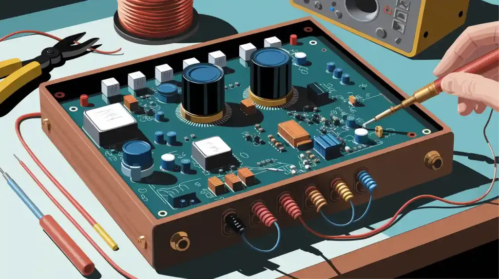
You use electronic design automation to make and check semiconductor chips. EDA helps you do jobs that would take a long time by hand. Chips have become much harder to make in the last ten years. Now, making chips needs over 1,000 steps. It takes about three months to finish. AI helps EDA work better and faster. Cloud technology lets you and your team work together from anywhere. The EDA market keeps getting bigger:
The global electronic design automation software market may reach USD 15.89 billion in 2026.
This is a big jump from USD 14.55 billion in 2025.
Experts think the market will be about USD 32.15 billion by 2034.
You can see how EDA tools help build strong and smart semiconductor chips today.
Key Takeaways
Electronic Design Automation (EDA) makes chip design easier. It helps people work faster and with fewer mistakes.
AI and cloud technology make EDA tools better. Teams can work together from anywhere. They can fix design problems quickly.
EDA tools help save money. They help chips work better and use less power.
Learning about new EDA tools is very important. The semiconductor industry changes all the time.
Using design for manufacturability helps make better chips. It means there are fewer problems and chips work well.
Electronic Design Automation Overview

What is Electronic Design Automation?
You use electronic design automation, or eda, to help make and check semiconductor chips. Eda gives you software, hardware, and services that make chip design easier. You do not need to draw every wire or check each part by hand. Instead, you use eda tools to plan, build, and check your designs.
Here is how top industry groups talk about electronic design automation:
Aspect | Description |
|---|---|
Definition | Eda is a group of software, hardware, and services that help with designing, making, checking, and building semiconductor devices. |
Role of EDA | Eda tools are important for designing and checking the chip-making process, making sure designs are right, and watching how chips work after they are made. |
Key Areas | 1. Technology Computer-Aided Design (TCAD) 2. Design for Manufacturability (DFM) 3. Silicon Lifecycle Management (SLM) |
Eda covers many steps. You start with planning and end by making sure your chip works after it is built. The eda market started in 1981. At first, big companies like Hewlett-Packard, Tektronix, and Intel used eda for their own work. The U.S. Department of Defense helped pay for VHDL, a language for describing hardware, in the early 1980s.
When you use eda, you follow steps to turn your idea into a real chip. Here is a simple list of the main stages:
Design planning: You set goals and limits for the chip.
Circuit design: You draw the main parts and decide how they work.
Circuit simulation: You test your design on a computer to see if it works.
Physical layout: You put the parts and wires on the chip.
Physical verification: You check that your layout follows the rules and matches your plan.
Timing analysis and optimization: You make sure signals move fast enough.
Power analysis and optimization: You check and improve how much power the chip uses.
Integration and verification: You put all the parts together and test the whole chip.
Physical manufacturing preparation: You get the chip ready to be made in a factory.
💡 Tip: Eda tools help you at every step, so you can focus on making better semiconductor chips instead of worrying about small details.
Why EDA Matters Today
Semiconductor chips are in almost everything you use. Phones, cars, computers, and even smart fridges need these chips. Today’s chips are much more complex than before. Some chips have over a billion tiny parts. You cannot design or check these by hand. You need eda to keep up.
Here is a table that shows why eda is so important for you and the whole eda market:
Key Reason | Explanation |
|---|---|
Complexity of Modern Chips | Today’s chips can have over a billion circuit elements, so you need advanced automation tools. |
Risk Management | Mistakes in making chips can cause big losses, so eda helps you avoid errors and finish projects. |
Market Pressures | The eda market moves fast. Eda tools help you work quickly and meet tight deadlines. |
New Process Technologies | Eda tools let you use the latest ways to make chips, helping the eda market grow. |
Eda is not just about making things easier. Eda helps you avoid mistakes and lets you use new technology. The eda market also helps you finish your work faster, which is important when everyone wants the newest devices.
When you use eda, you also get better results. In recent years, the eda market has seen big improvements:
Metric | Improvement |
|---|---|
Cost of code generation | Reduced by 89.6% |
Success rates | Improved by 5.8% |
Power consumption | Reduced by 24.5% |
Pass rates on RTLLM benchmark | Increased by 24.0% |
You save money, use less power, and make fewer mistakes. The eda market helps you build better semiconductor chips, which means better products for everyone.
The eda market keeps growing because you and other designers need faster, safer, and smarter ways to make semiconductor chips.
Eda tools let you work with teams around the world, thanks to cloud technology.
You can use artificial intelligence in eda to find problems and fix them before they become big issues.
📝 Note: The eda market is always changing. If you want to stay ahead, you need to learn about new eda tools and how they help you design the next generation of semiconductor chips.
EDA Evolution and Technology Shifts
From Manual to Automated Design
Long ago, engineers drew chip diagrams by hand. This took a lot of time and caused mistakes. Chips got harder to design as they became more complex. Manual work could not keep up anymore. EDA changed everything for engineers. You started using software to do many steps for you. Now, you can spend more time on new ideas. By the early 2000s, EDA helped you work faster and make fewer errors. You could design chips with millions of parts. This was not possible before. Automation made your work better and more exact.
EDA tools can make design time shorter by 30%. You finish projects faster and meet your deadlines.
AI-powered design space exploration can cut down cycles by 25%. You get products ready for sale sooner.
Pilot programs show a 15% drop in design costs. You save money and make better designs.
Tip: Automated design helps you avoid mistakes and gives you more time to invent new things.
AI and Cloud in EDA
Today, AI and cloud technology have changed EDA a lot. AI helps you look at many design choices quickly. You find the best ones faster. For example, Synopsys DSO.ai makes chips use less power and work better. Cadence Cerebrus AI makes chip design five times faster. Siemens EDA AI System helps you work ten times faster and finish chips three times quicker.
AI Tool | Key Features and Improvements |
|---|---|
Synopsys DSO.ai | Makes chips use less power and work better. Used in over 100 chips. |
Cadence Cerebrus AI | Chip design is five times faster, and it can optimize many blocks at once. |
Siemens EDA AI System | Ten times more work done, three times faster chip finishing. |
Cloud computing lets you and your team work together from anywhere. You upload your designs and pick the tools you need. You run tests in the cloud. The cloud gives you all the computer power you need. You see changes right away and share results fast. Cloud EDA makes teamwork easy and grows with your project.
Better teamwork: You and your team can edit projects together.
Scalability: You can use more computer power for hard jobs.
Flexibility: You get storage and tools when you need them.
Note: Using EDA in the cloud gives you quick access to strong tools and helps you work with teams all over the world.
Core EDA Tools and Functions
Simulation and Verification
Simulation and verification help you check your chip ideas. You use these steps before building anything. Simulation lets you see how your chip acts in different cases. You can test analog and digital circuits. You also check timing and power use. Verification makes sure your chip follows the rules and works right. You use things like formal verification and signal checks to find mistakes early.
Here is a table that shows what simulation and verification do in electronic design automation:
Function | Description |
|---|---|
Simulation | Lets you test how circuits work in many ways, like analog and digital tests, timing checks, and power checks. |
Verification | Makes sure your design meets the rules and works as it should by using formal checks, tests, and signal checks. |
Simulation and verification tools help you spot errors before making chips. You can:
Look at your design closely before building.
Test your chip in many situations.
Change your design to fix problems.
Use real data to guess how your chip will work.
These tools help you save time and money. You do not need to redo work or waste parts. You get better chips and fewer surprises.
Design for Manufacturability
Design for manufacturability helps you make chips that factories can build easily. This step lowers the chance of defects and makes things smoother. You use special ways to help your design fit what factories need.
Here is a table that shows some common ways you use in design for manufacturability:
Technique | Description |
|---|---|
Redundancy | Add extra parts to important paths, so if one fails, the chip still works. |
Fill patterns | Put shapes in empty spots to make patterns better and cut down on changes during making. |
Optical proximity correction (OPC) | Change mask shapes to fix problems that happen when making chips. |
Restricted design rules (RDR) | Use stricter rules to make chips easier to build. |
Yield simulations | Use math models to guess how changes affect how many good chips you get, so you can change your design. |
These ways help you avoid common chip problems. Bad designs can cause more defects and extra work. If you use these ways, you get fewer defects and save money. For example, one factory had 9% fewer defects in ten weeks after using these steps. Big companies like Toyota use these ideas to get zero defects and work better.
🛠️ Tip: Using design for manufacturability makes your chips easier to build and more dependable.
Improving Chip Quality
You want your chips to last and work well. EDA tools help you reach this goal. You use design and checks to look at every part of your chip. You use simulation to see how your chip will act. You use checks to make sure your chip will not break in real life.
EDA tools help with reliability and performance. You use good steps from start to finish. You collect data and use AI to find problems early. You can fix issues before they get big. As chips get better, mistakes cost more. EDA tools help you avoid mistakes by letting you test everything first.
Here is a table that shows how EDA tools help with reliability and performance:
Evidence | Explanation |
|---|---|
Reliability best practices must be used in design, making, and testing. | EDA tools help keep chips reliable by using good steps in every part of making chips. |
Simulation matters more as mistakes get costly. | EDA tools help you do deep tests to stop expensive errors in new chips. |
Real-time data and AI/ML can help with chip reliability and aging. | EDA tools now use smart tech to make chips last longer and work better. |
EDA tools help you make chips that are strong, safe, and ready for new uses. You can trust your chips in phones, cars, and computers. You can also keep up with new tech and make better products.
✅ Note: Using EDA tools for design and checks helps you build better chips and helps your company win.
Common EDA Tools
You use many tools in electronic design automation. Each tool helps with a different part of chip design. Some tools help you test ideas. Other tools help you draw the chip. Some tools check if your chip works right. Let’s see which tools you might use most.
Simulation Tools
Simulation tools let you test your chip before building it. You can see how your chip acts in different cases. These tools help you find mistakes early. You can fix problems before they cost a lot.
Here is a table that lists top simulation tools and what makes them special:
Tool | Key Features | Why You Should Use It |
|---|---|---|
ModelSim | Supports behavioral and gate-level simulation, strong debugging capabilities. | Free student version, great for mini projects, prepares you for industry. |
Xcelium | Powerful simulation for complex designs, supports mixed-signal verification. | Gives you real-world VLSI experience, ideal for advanced projects. |
VCS | Extremely fast simulation, supports advanced SystemVerilog features. | Builds industry-relevant skills, best for verification roles. |
You use simulation tools for both easy and hard designs. ModelSim is good for learning and small projects. Xcelium is best for big, mixed-signal designs. VCS is fast and has advanced features for large systems.
💡 Tip: Try out different simulation tools to find the best one for your project.
Layout Tools
Layout tools help you draw the chip’s parts and wires. You use these tools to make sure your design fits and works. Each tool is good at something special.
Here is a table that shows how popular layout tools compare:
Tool | Best For | Key Features |
|---|---|---|
Virtuoso | Full-custom, high-volume analog/MS SoCs | Deep integration for schematic, layout, simulation, and verification; strong visualization; foundry support |
IC Compiler | Digital place-and-route | Automates placement of gates and cells, optimizes for timing, area, and power |
Tanner EDA | Cost-sensitive teams and education | Easy to use, combines capture, simulation, and layout; good for small to mid-sized teams |
Virtuoso is great for custom analog and mixed-signal chips. IC Compiler is best for digital designs and helps everything fit and run fast. Tanner EDA is simple to learn and good for schools or small teams.
🛠️ Note: Good layout tools help you avoid mistakes and make your chip easier to build.
Verification Tools
Verification tools help you check if your chip works as planned. You use these tools to find hidden bugs and make sure your design follows all rules. Some tools use math to check every possible case, not just the ones you test in simulation.
Formal verification uses math to prove your design is correct. It checks every possible condition and finds bugs you might miss with other tests.
JasperGold uses static analysis and model checking. It finds problems early and helps you fix them before you build the chip.
Questa gives you a full environment for both functional and formal verification. Many companies use QuestaSim and VCS to check their designs.
✅ Tip: Use verification tools to make sure your chip is safe and ready for real-world use.
Each tool has a special job. Simulation tools help you test ideas. Layout tools help you draw and build the chip. Verification tools help you check for mistakes. When you use the right tools, you make better chips and learn skills that companies want.
Leading EDA Tools in Practice
Cadence and Industry Solutions
Cadence tools help you with every part of chip design. You start with an idea and end with a working chip. These tools work well with other platforms. You finish your projects faster and make fewer mistakes. You can use one tool for simulation. Another tool helps with layout. A different tool checks your work. This makes your job easier. You avoid errors and save time.
Here is a table that shows how Cadence tools help with each chip design step:
Cadence Product | Description |
|---|---|
Spectre X Simulator | Strong circuit simulator for analog and mixed-signal designs |
Xcelium Logic Simulation | Fast platform for checking digital designs |
Helium Virtual and Hybrid Studio | Platform for software development and testing before making chips |
Liberate Trio Characterization | Tool for cell libraries and memory checks |
Jasper Formal Verification | Platform to make sure designs are correct |
Innovus Implementation System | Advanced system for building integrated circuits |
Genus Synthesis Solution | Solution that turns RTL code into gate-level netlists |
Joules RTL Design Studio | Accurate tool for checking power use |
Quantus Extraction Solution | Trusted tool for cell and transistor extractions |
Cadence gives you many eda tools. These tools help with simulation, checking, layout, and power tests. You can trust these tools to work with other platforms. They help you build better chips.
Real-World Impact of EDA Tools
EDA tools show their value when companies use them. These tools help you solve tough problems. They let you make new things. Here are some examples of how eda and ai change chip design:
You can check designs better. Big companies use eda tools with ai to automate checks. This cuts errors by up to 30%. You finish designs faster.
You can make chips use less power. AMD uses advanced eda tools to boost performance-per-watt. You can lower power use by 20% and keep speed.
You can join open-source projects. The OpenROAD Initiative lets over 120 developers use eda tools. They explore new chip designs. More people learn and create in the chip industry.
EDA tools help you work faster and safer. You can use ai to find problems early. You fix issues before they waste time or money. These tools help you keep up with new technology.
💡 Tip: When you use eda tools, you join engineers who shape the future of electronics.
You see how electronic design automation helps you design and build better semiconductor chips. EDA makes your work faster and more accurate. AI and cloud technology change how you use EDA tools. You get smarter design checks and faster results. Cadence and other leaders shape the future of EDA. You can expect these trends in the coming years:
EDA will grow as chip designs get harder.
AI and cloud will help you solve problems and save time.
More teams will use EDA for new semiconductor chips.
To stay ahead, you should:
Check if your EDA vendor gives good support.
Make sure your tools follow rules and standards.
Test new EDA solutions before using them for all your semiconductor chips.
📝 Stay curious and keep learning about EDA. You will help build the next generation of semiconductor chips.
FAQ
What does EDA stand for?
EDA stands for Electronic Design Automation. You use EDA tools to help design, test, and build semiconductor chips. These tools make your work faster and more accurate.
Why do you need EDA tools?
You need EDA tools because chips are too complex to design by hand. EDA tools help you avoid mistakes, save time, and create better products.
Can you use EDA tools on the cloud?
Yes! You can use EDA tools on the cloud. Cloud EDA lets you and your team work together from anywhere. You get more computer power and faster results.
Which EDA tool should you learn first?
Tool | Best For |
|---|---|
ModelSim | Beginners, students |
Virtuoso | Analog design |
VCS | Digital design |
You should start with ModelSim if you are new. It is easy to use and helps you learn the basics.
How does AI help in EDA?
AI helps you find problems in your chip design faster. You can use AI to test many ideas quickly. This makes your work easier and helps you build better chips.