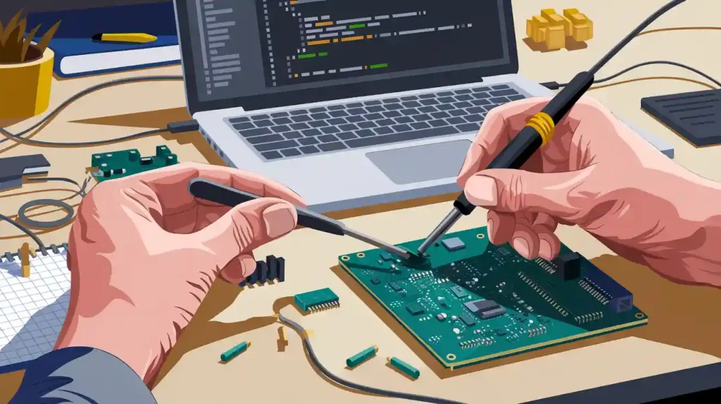
Custom WiFi PCBs are changing IoT devices
These devices will create over 79.4 zettabytes of data.
They will also be more than half of all connected devices.
Good PCB design is very important for IoT devices.
About 85% of IoT devices use batteries for power.
Custom designs make devices work better and cost less.
They solve problems like small size and limited power.
Wearable health monitors are one example of custom PCBs.
Industrial IoT gateways also use these special PCBs.
Custom PCBs help devices stay small, fast, and reliable.
Designing a WiFi PCB opens new ideas for IoT devices.
Key Takeaways
Know what your IoT device needs before making a WiFi PCB. Think about size, power use, and where it will be used.
Pick the right WiFi module or chip for good performance. Make sure it fits your device’s needs for the best results.
Use parts that save power and designs that reduce heat. This helps batteries last longer in IoT devices.
Try tools like KiCad or Altium Designer to design PCBs easily. These tools make designing faster and more accurate.
Learn about new WiFi tech and green practices. This helps your designs work well in the future and stay eco-friendly.
Planning for a Custom WiFi PCB
Understanding IoT Device Needs
Before making a custom WiFi PCB, know your IoT device’s needs. Think about what the device does and where it will be used. For example, small wearables need tiny designs, while industrial devices must handle tough conditions.
Important things to consider are:
Miniaturization: Make sure the PCB fits in the small space.
Low Power Consumption: Save energy to make the battery last longer.
Wireless Connectivity: Ensure strong WiFi for smooth communication.
Environmental Resilience: Build it to work in heat or wet places.
Security Features: Add hardware security to keep data safe.
By focusing on these, you can design a PCB that works perfectly for your device.
Picking the Best WiFi Module or Chipset
Choosing the right WiFi module or chipset is very important. Look at these points to decide:
Criteria/Metric | What It Means |
|---|---|
Data Rate Needs | High data rates are for videos; sensors need less. |
Microprocessor/Microcontroller Compatibility | The WiFi module must work well with the MPU/MCU. |
Operating System Support | It should match the operating system for easy use. |
Physical Characteristics and Environmental Conditions | The module must fit and work in the expected environment. |
Picking a module that matches your device ensures it works well and lasts long.
Solving IoT Problems Like Power and Size
IoT devices often struggle with power and size limits. Here are ways to fix this:
Use low-power parts like special microcontrollers and sensors.
Add sleep modes to save energy when not in use.
Improve power use with smart regulators and power-saving tricks.
Design layered PCBs to fit more parts in less space.
Use thermal vias and copper to handle heat better.
These tips help you make a small, energy-saving WiFi PCB for today’s IoT needs.
Circuit Design and Simulation for IoT
Using tools like KiCad and Altium Designer
To design WiFi PCBs, you need good software tools. KiCad and Altium Designer are two great options. KiCad is free and open-source, so anyone can use it. It lets you make multi-layer designs and check for errors. You can also see 3D views of your layouts. Altium Designer has advanced features like checking signal quality and managing layers. Its easy-to-use interface helps with big projects. It’s great for adding Arduino systems to industrial IoT devices.
Software | Advantages |
|---|---|
Altium Designer | – Easy to use for complex designs. |
– Lets teams work together on big projects. | |
– Has tools for signal checks and layer management. | |
KiCAD | – Free and open for everyone. |
– Big community helps improve the software. | |
– Offers 3D views, multi-layer support, and error checks. |
These tools make designing WiFi PCBs easier and better for IoT devices.
Integrating WiFi modules into schematics
Adding WiFi modules to your PCB needs careful planning. Make sure they work well with microcontrollers like Arduino. This avoids problems with signals and power. Keep signal paths short to reduce interference. Use shielding to protect signals from noise. Place antennas in the right spot for better wireless performance.
Design Strategy | Description |
|---|---|
Controlled Impedance Routing | Keeps signals clear by managing trace impedance. |
Signal Shielding | Blocks noise to keep signals strong and clear. |
Minimizing Signal Trace Lengths | Shorter paths mean better signal quality. |
Proper Antenna Placement | Helps signals send and receive better. |
RF Signal Isolation | Stops noise from affecting the wireless parts. |
Impedance Matching | Makes energy transfer between antenna and PCB efficient. |
By following these steps, your WiFi PCB will work well in many IoT settings.
Simulating circuits for functionality and performance
Testing your design is very important. Tools like HyperLynx and Ansys SIwave check signal quality. Icepak and FloTHERM find hot spots in your design. Power analysis ensures steady power flow. Rule checks make sure your design can be built. For Arduino IoT devices, test all modes to ensure they work.
Simulation Technique | Purpose |
|---|---|
Signal Integrity Simulation | Checks signal quality with tools like HyperLynx. |
Power Integrity Analysis | Ensures power flows steadily. |
Thermal Simulation | Finds hot spots in your design. |
Design Rule Checks | Makes sure the design can be built. |
EMI and RF Analysis | Checks for noise issues. |
Design Data Review | Confirms the design meets all needs. |
Modern software also has auto-routing and impedance tools. These improve signal and heat performance. Testing early helps fix problems and makes your WiFi PCB better for IoT.
Optimizing PCB Layout for WiFi
Keeping WiFi Signals Strong and Antenna in the Right Spot
Strong WiFi signals are key for IoT devices to work well. Use methods like controlled impedance routing and signal shielding. These help block noise and keep signals clear. Shorter signal paths also improve performance by reducing signal loss.
For antennas, place them at a corner of the PCB. This gives space in five directions and avoids nearby parts. Keep the gap between CPWG grounds smaller than the substrate height. This boosts signal strength. These steps make your WiFi PCB work better, especially in small IoT devices like Arduino systems.
Saving Power and Managing Heat
Saving power and controlling heat are very important for IoT devices. Use low-power parts and add sleep modes to save energy. Smart regulators and power-saving tricks help batteries last longer in devices like Arduino wearables.
To stop overheating, design the PCB to spread heat evenly. Use extra PCB layers, thermal vias, and copper pours to cool it down. These ideas keep your WiFi PCB working well in different environments, perfect for IoT use.
Making Small Layouts for IoT Devices
Small layouts are needed because IoT devices have little space. Place parts smartly in 2-D or 3-D to save time. Manage space well so the PCB fits inside the device without losing features.
Aspect | What It Means |
|---|---|
Component Placement | Place parts quickly in 2-D or 3-D while following rules. |
Constraint Management | Handle space limits to make small PCBs for IoT devices. |
Thermal Management | Use heat control methods to keep devices reliable. |
High-density layouts improve signals and reduce noise. Use controlled impedance routing and shielding to keep performance strong. Small designs also save energy, making them great for IoT systems.
Prototyping and Testing WiFi PCBs
Quick prototyping for IoT PCBs
Quick prototyping is key for making custom WiFi PCBs. It helps turn ideas into working models fast. This speeds up the process and meets tight schedules. It also saves money by fixing mistakes early.
Here’s why it’s helpful:
Benefit | What It Means |
|---|---|
Faster Development | Turns ideas into prototypes quickly, helping you stay ahead. |
Lower Costs | Fixes mistakes early without spending too much money. |
Better Design Accuracy | Makes sure designs are copied correctly, avoiding big errors. |
More Creativity | Lets you try new materials and layouts for better ideas. |
Early Testing | Tests the design early to make sure it works well. |
Using quick prototyping improves your design and gets your WiFi PCB ready for IoT use.
Checking signal strength and rules
Testing makes sure your WiFi PCB works in real life. Check signal strength, power use, and if it follows rules. Use tools like spectrum analyzers to find problems with signals. Test the PCB in different places to check its connection.
Following rules is also important. It ensures your PCB meets standards for noise and wireless signals. This is crucial for devices like Arduino IoT systems that work in busy wireless areas.
Improving designs after testing
Testing shows how to make your design better. If signals are weak, move the antenna or fix the layout. For heat problems, add thermal vias or improve cooling. Always update your design based on test results.
For Arduino IoT devices, make sure the PCB does everything it needs to. It should stay small and use little power. Improving your design after each test ensures your WiFi PCB fits modern IoT needs.
Manufacturing and Assembly of IoT PCBs
Picking trustworthy manufacturers and assembly services
Choosing a good manufacturer is key for making great WiFi PCBs. Pick companies with experience in small designs and low-power parts. Look for those using advanced methods like surface-mount technology (SMT) for better accuracy.
Check if the manufacturer has certifications like ISO 9001 for quality. A good partner will also communicate clearly and help during production. This ensures your design becomes a working product without mistakes.
Finding parts for IoT devices
Getting the right parts is important for your IoT PCB to work well. Always buy from trusted suppliers to avoid fake parts. Make sure each part fits your design to avoid problems.
Choose parts that save power and are small, as IoT devices need these. For example, pick energy-saving microcontrollers and sensors. If your device will face heat or moisture, use parts that can handle tough conditions.
Checking quality during production
Quality checks are very important to make sure your IoT PCB works well. Use different tests during production to find problems early.
Test Type | What It Does |
|---|---|
In-Circuit Testing (ICT) | Checks if all connections work. |
Functional Testing (FT) | Makes sure the PCB does its job. |
Environmental Stress Testing (EST) | Tests if it can handle tough conditions. |
Besides testing, use strong quality control steps. Automated checks like DRC and DFM can spot issues before production. Inspect parts to ensure they are real and good quality. Tools like AOI and X-ray can find missing parts or hidden flaws.
To improve results, use real-time data and smart quality tools. IoT sensors can track production, and machine learning can predict problems early. These steps make sure your PCB is ready and reliable for IoT use.
Future Trends in WiFi PCB Design
New WiFi Technologies for IoT
New WiFi types are solving IoT problems like range and power. Wi-Fi HaLow is a big improvement for IoT devices. It works over long distances and uses less power. This makes it great for battery-powered gadgets. For example, smart cameras can now be far from routers and still work well. This helps them cover large areas better.
Wi-Fi 7 is another exciting update with faster speeds. It uses multi-link operation (MLO) to connect on many bands at once. This keeps devices working even in busy homes with lots of gadgets. Wi-Fi 7 also has 4K-QAM, which sends more data for things like videos. Better security features protect devices from hackers, making them safer to use.
These WiFi updates make IoT devices smarter and more useful. They keep devices connected, safe, and ready for modern needs.
Green Practices in PCB Making
Making PCBs is becoming more eco-friendly. Many factories now use recycled copper and materials that break down naturally. These choices follow strict rules and attract eco-friendly buyers. Using green methods also helps companies look better to customers.
Eco-friendly ways cut waste and save energy during production. This is important as more IoT devices need PCBs. Choosing green materials and methods helps the planet while making new IoT devices.
Getting Ready for IoT Changes
IoT devices will need better WiFi PCBs in the future. Smarter devices will need PCBs that handle more data and work faster. To prepare, learn about new WiFi types like Wi-Fi 7.
PCBs must also support many devices as IoT networks grow. Adding strong security will stay important as hacking risks increase. By planning for these changes, you can make PCBs ready for future IoT needs.
Making a custom WiFi PCB for IoT devices has key steps. First, know what your device needs and pick the right WiFi module. Solve problems like saving power and fitting in small spaces. Use tools like KiCad or Altium Designer to design and test circuits. Arrange parts smartly for strong signals, low power use, and small size. Build, test, and improve your design to make it work well. Pick good manufacturers and buy quality parts for smooth production.
💡 Tip: Use smart tools to make designing easier. Test early to fix problems fast.
Learn about new trends like Wi-Fi 7 and green methods. These help you make better designs for the future. By following these steps, your IoT devices will be powerful and efficient.
FAQ
What matters most when designing a WiFi PCB for IoT?
Focus on keeping signals strong and saving power. These make sure the device connects well and the battery lasts longer, which are key for IoT gadgets.
Can I use free tools to design a WiFi PCB?
Yes, free tools like KiCad work great. They have features like multi-layer designs, error checks, and 3D views, making them good for IoT projects.
How do I make sure my WiFi PCB follows rules?
Follow design rules for clear signals, low noise, and good heat control. Test your PCB with tools like spectrum analyzers and check it meets standards like FCC or CE.
What’s the best way to test a WiFi PCB?
Try quick methods like 3D printing or PCB milling. These let you test your design fast and fix problems before making more.
How can I save power in my IoT PCB?
Pick parts that use less power, add sleep modes, and use smart power regulators. These steps help batteries last longer in IoT devices.