When you start PCB reverse engineering, you meet real problems at every step. You may see old boards without documents or with many layers. These are some common problems you will face when you do manual pcb reverse engineering:
You often have trouble with pcb analysis because there are no original papers.
Multi-layer pcb designs make it hard to follow connections.
You see faded part numbers, so it is hard to know the parts.
Old boards make you look for parts that are not made anymore.
Time and money can make things more stressful for you.
A hands-on guide helps you learn faster and fix problems as you work.
Key Takeaways
Pick a PCB project that matches your skills. Begin with easy boards to help you feel confident and learn more.
Make sure you know what you want to do before you start. Having clear goals helps you stay on track and see how much you have done.
Write down everything you find. Take good notes and pictures so you can remember details and show your work to others.
Use the best tools for your project. Try out different software and hardware to see what works well for you.
Work slowly and carefully. Take your time with each step because careful work gives you better results in reverse engineering.
Choosing PCB Reverse Engineering Projects
Project Selection Criteria
You want to pick the right project before you start pcb reverse engineering. Not every pcb is a good fit for your skills or your tools. You should look for boards that match your experience level. If you are new, try a simple pcb with clear traces and easy-to-find parts. If you have more experience, you can choose a board with more layers or a unique design.
Here are some things you can check before you decide:
Board Complexity: Is the pcb single-layer or multi-layer? Simple boards help you learn faster.
Component Availability: Can you find the parts used on the pcb? Old boards may have rare or obsolete parts.
Documentation: Does the pcb come with any manuals or diagrams? If not, you will need to do more detective work.
Purpose: Does the pcb serve a function you care about? Projects that interest you keep you motivated.
Tip: Start with a project that excites you. You will learn more and enjoy the process.
Setting Objectives
You need clear goals before you begin pcb reverse engineering. Ask yourself what you want to achieve. Do you want to repair a broken pcb? Maybe you want to clone a design or learn how it works. Setting objectives helps you stay focused and measure your progress.
Try writing down your main goal. Here is a simple table to help you organize your thoughts:
Objective | Example |
|---|---|
Repair | Fix a broken audio amplifier |
Clone | Make a copy of a vintage pcb |
Learn | Understand signal flow |
When you know your goal, you can plan each step. You will save time and avoid mistakes. Remember, every pcb reverse engineering project teaches you something new.
Reverse Engineering Process Steps
Initial PCB Assessment
When you begin, look at the pcb very carefully. This helps you see how hard the board will be to work on. You need to find out how many layers the pcb has. Count the number of parts on the board. Look at the different package types you see. Check if there are shields or any security features. This step helps you know what you are working with.
Here’s a simple table that shows the main ways to check the pcb:
Technique Type | Techniques |
|---|---|
Board Complexity | Count layers, estimate component count, identify package types, note shielding features, check for security features |
Functional Context | Identify system association, input/output connections, power requirements, interface specifications |
Try to figure out what the pcb does. Look at the connectors and see what kind of power it needs. Guess what the circuit does by checking the input and output spots. This helps you plan your next steps and pick the right tools.
Tip: Take clear photos of the pcb before you start. Good pictures help you remember where each part goes and make your work easier.
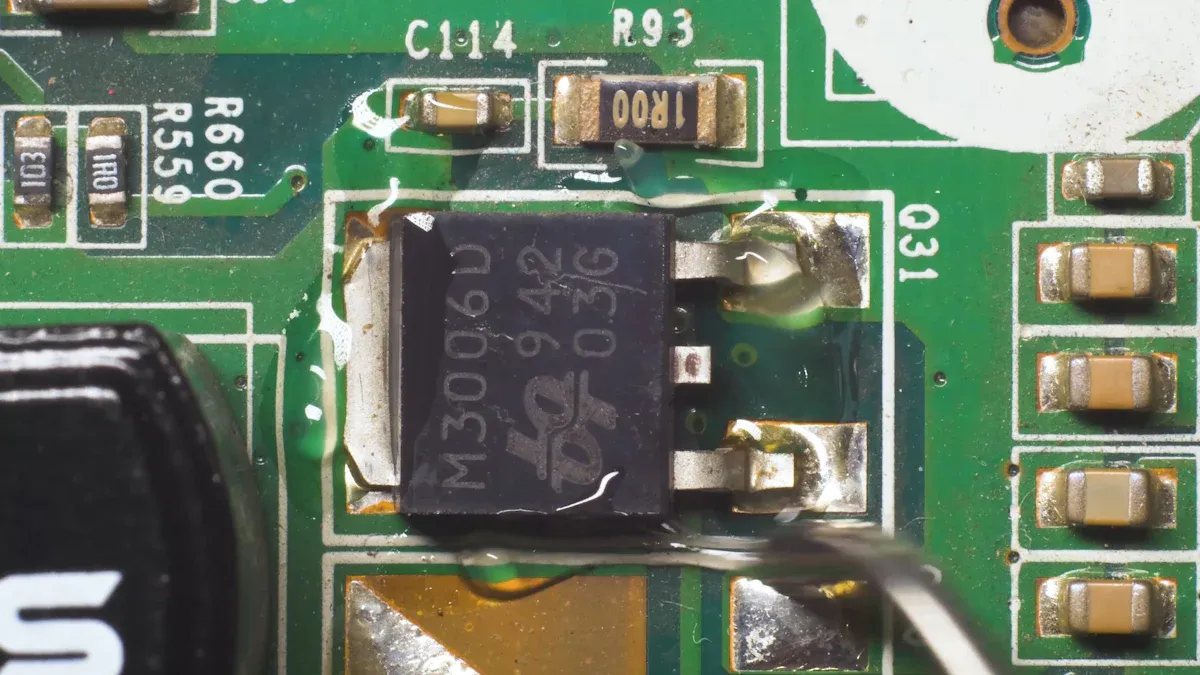
Examining Connectors and Traces
Next, look closer at the pcb. Start with the connectors. These are where signals and power go in and out. Follow the traces from the connectors to see where they lead. This helps you map the circuit and see how things connect.
Here’s a step-by-step list to help you:
Make sure your workspace is bright and use magnifiers.
Clean the pcb if it is dirty.
Look at the whole board and notice the main areas.
Find important parts using their labels.
Trace the power and ground lines first.
Follow signal paths from input to output.
Look closely at microcontrollers, memory chips, and power regulators.
Check solder joints and leads for any damage.
Look for cracks or burns on the pcb.
Compare what you see with any schematic you have.
Write down any problems or questions you find.
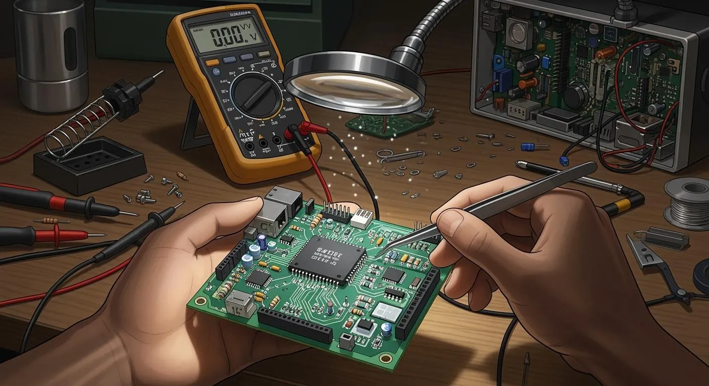
Use a multimeter to check if two points are connected. Set it to continuity mode and turn off the power. Put the probes on two spots. If you hear a beep or see low resistance, the connection is good. Do this for other traces to finish your check.
Some pcb reverse engineering tools can help you. You can show or hide layers, highlight nets, search for parts, measure spaces, and link symbols to footprints. These tools make your work faster and more correct.
Note: Always start with connectors. They help you map the board step by step and make the process easier.
Creating a Rough Schematic
After you finish checking connectors and traces, make a rough schematic. This is one of the hardest steps. You need to draw the circuit diagram from what you see. Sometimes there are no papers, so you must use your own notes.
Here’s a table that shows the main steps:
Step | Description |
|---|---|
Preparation | Get your tools ready and make sure the pcb is clean and safe to handle. |
Schematic Generation | Draw a detailed diagram of all electrical connections and components on the pcb. |
Bill of Materials (BOM) | Make a list of every part used in the pcb, including specs and quantities. |
Start your schematic with the connectors and big parts. Draw the power and ground lines first. Then add the signal paths and other parts. Use your notes and photos to help you. If you see missing or broken parts, mark them on your drawing.
You might need software tools to help you. Some tools let you highlight nets, search for parts, and measure spaces. These tools make it easier to build your schematic and check your work.
Callout: Making a schematic from a pcb takes time. Don’t rush. Check your work and make sure every connection is right.
The reverse engineering process teaches you a lot about circuits and pcb layout. Each step helps you learn how the board works and how to fix or copy it. You will get better at analysis and engineering with every project you do.
Printed Circuit Board Documentation
Visual Inspection and Photography
Always begin by looking closely at the pcb. This helps you find scratches, dirt, or parts that look wrong. Sometimes, small problems are hard to see. Go slowly and check each part of the board. Break your work into small sections. Take a short break every thirty minutes. This helps your eyes and keeps you focused.
Taking pictures makes things easier. Use a camera with at least 10 megapixels. Take close-up photos of model numbers and polarity marks. These photos help you remember where parts go. If you have a schematic, compare it to your pictures. Make sure all the parts match up. Here is a table to help you with your photos:
Requirement | Details |
|---|---|
Camera Resolution | ≥10 megapixels |
Key Areas to Photograph | Component model numbers and polarity marks |
Tip: Be patient and check each area carefully. Good photos and notes help you avoid mistakes later.
Documenting Layers and Components
You need to keep good records when working on printed circuit boards. Writing things down helps you and your team remember each step. Write what you find, why you made choices, and how you fixed problems. This makes your pcb reverse engineering project better.
Start by measuring the board and counting the layers. Use a ruler or calipers to check the size. Look at the edges or use tools to see how many layers there are. Take photos from different sides of the board. Make a list of every part, including values and where you found them. Update your notes if you change something or find new details.
Draw pictures for making and putting together the board.
Add steps for fixing or changing parts.
List the order of layers and drill spots.
Keep a Bill of Materials with part details and amounts.
Note: Clear records help you share your work with others. Good communication is important for pcb reverse engineering.
Tools and Techniques for PCB Reverse Engineering
Essential EDA Tools
You need special tools for pcb reverse engineering. These tools help you look at circuits and see how things connect. Some tools let you draw pictures of the circuit. Other tools help you find mistakes in your work. If you want to go faster, try automated pcb reverse engineering tools. These tools can follow connections and find errors for you.
Here are some tools you might use:
Altium Designer can trace connections and check for mistakes.
Cadence OrCAD helps you draw circuit diagrams and connect parts.
Mentor Graphics PADS checks your design and makes strong diagrams.
You can also use KiCad, Eagle, EasyEDA, or OrCAD to draw and change circuits. These tools make pcb reverse engineering easier. They help you learn from guides and share your work with friends.
Tip: Try out different tools to see what you like best. Some tools are good for easy boards. Others work better for hard projects.
Hardware and Software Methods
There are many ways to study a pcb and its circuit. Some ways use computer programs. Other ways need special hardware. You can pick what works best for your project.
Here’s a table that shows some common ways and tools:
Category | Tools/Techniques |
|---|---|
PCB Design Software | KiCad, Altium Designer, Eagle, EasyEDA, OrCAD |
Simulation Tools | LTSpice, ngspice, Falstad Circuit Simulator, TINA-TI |
Non-Destructive Methods | X-ray Tomography |
Destructive Methods | Delayering (sandpaper abrasion, chemical etching, CNC milling) |
If you do not want to hurt the pcb, use X-ray tomography. This lets you look inside the board and see hidden paths. For hard jobs, you may need to take apart the pcb with sandpaper or chemicals. This helps you see each layer and follow every connection.
Automated pcb reverse engineering saves you time. You can finish hard boards in weeks, not months. This is good if you need to finish projects fast and keep your work correct.
Note: Always choose the safest way first. Use computer tools and safe methods before you try risky ones.
PCB Reverse Engineering Challenges
Multi-layer and Hidden Interconnections
Not every pcb is simple to understand. Multi-layer boards can be tricky. Many projects have boards with hidden connections inside. You cannot see these traces just by looking. You need special ways to find them.
Internal layers are hard to see, so you need advanced tools.
You can use careful sanding or chemicals to separate layers.
High-resolution pictures help you spot tiny things.
Matching up layers helps you see how they fit together.
Some boards have blind and buried vias. These are hard to find. You need good imaging and careful separation to see them.
HDI pcbs have very complex parts. You need patience and the right tools. Sometimes, you use X-ray pictures to look inside the board. This helps you find every connection and learn how the pcb works.
Tip: Start with the outside layers first. Work slowly inward. Use special tools when you need to see hidden parts.
Missing or Obsolete Components
You may find missing or old parts when you do reverse engineering. Old pcbs often use parts that are hard to get now. Sometimes, you cannot read the part numbers because they faded.
Engineers use machines with cameras to find parts fast. Machine vision helps you spot resistors, capacitors, and other parts. If you find an old part, you can look for a new one. This keeps the pcb working and lets you fix or upgrade the board.
Machines with cameras find parts quickly.
Machine vision helps you pick the right parts, even if they look alike.
Reverse engineering lets you choose cheaper replacements for old parts.
If you cannot find the exact part, do not worry. You can use your skills to pick a new part that works well.
Note: Always check replacements to make sure they work like the original.
Cost and Proprietary Designs
Money and secret designs can make reverse engineering hard. You need to think about cost and rules before you start. Some pcbs use special parts or secret layouts. You need to find ways to solve these problems.
Cost analysis shows how others pick parts and design boards. You can use this to save money.
You need to find problems like old parts and secret components early. This helps you plan and avoid surprises.
Legal rules matter. You should follow clean room steps and keep good notes.
You can make plans and add extra time to your project. This helps you deal with hard designs.
Strong rules and legal checks help you stay safe on tough projects.
Some fields, like healthcare and aerospace, have strict rules. You need to follow these when you do reverse engineering.
Engineers use smart ideas to beat secret design problems. Here is a table with some good ways:
Technique | Description |
|---|---|
Advanced Imaging | X-ray pictures help you see inside multi-layer pcbs, but you need special skills. |
Iterative Testing | You test the pcb in small steps to check if it works. |
Thorough Documentation | You keep good notes and photos. This helps you review designs and share ideas with your team. |
You can use these ways to fix problems and keep your project going. If you stay organized and use the right tools, you can handle almost any challenge.
Callout: Do not let cost or secret designs stop you. With smart planning and creative ideas, you can figure out any pcb.
Lessons and Real-World Examples
Practical Tips and Best Practices
You can learn a lot from real pcb engineering stories. When you start a pcb project, you need good tools and a smart plan. Here are some tips to help you do well:
Get all your tools ready and clean the pcb first. This keeps your area safe and stops dirt from causing problems.
Split the job into small steps. You will make fewer mistakes and finish faster.
Use new resources and technology. Better tools help you find hidden connections and get better results.
Check your work after each step. Testing helps you find problems early.
Follow rules and respect intellectual property. This keeps your project safe and legal.
Write notes and take pictures. Good records help you share your work and learn from real examples.
Work on one part at a time. You will stay organized and not get confused.
Ask experts for help if you need it. Working together brings new ideas and tools.
Test the pcb in real situations. This makes sure your repair or design works right.
Tip: Always write down what you do. You will be glad later when you need to look back at your pcb engineering steps.
Case Studies and Outcomes
You can see how these tips help in real projects. One company had to reverse engineer many fiber gaskets for cooling machines. They did not have enough skilled workers and had little money. By using smart tools and careful planning, they measured and studied each gasket. The project worked better and saved money.
Sometimes, things do not go as planned. Here is a table with lessons from failed pcb engineering projects:
Category | Description |
|---|---|
Physical damages | Devices can break from water, dust, drops, or heat. |
Manufacturing errors | Small mistakes in making the pcb can cause big problems. |
Component failures | Old parts can stop working and need pcb repair. |
Design flaws | Wrong part placement can make the pcb fail or work poorly. |
You can use these lessons to stop problems in your own pcb engineering work. Real examples show that good tools, teamwork, and careful planning lead to better results.
You can do well in PCB reverse engineering if you ask questions and write things down. Here are some things to remember:
Lesson/Advice | Description |
|---|---|
Stay Curious | Always wonder about things and try new ideas. |
Documentation | Write notes and take pictures to remember your steps. |
Structured Processes | Make a simple plan to help you work and choose. |
Keep learning new things and try using better tools. Follow good habits and obey the rules. When you change and learn, your projects get better and work well.
FAQ
What is PCB reverse engineering?
You take apart a printed circuit board to learn how it works. You follow traces, identify parts, and draw a new schematic. This helps you fix, copy, or improve the board.
Do I need expensive tools to start?
No, you can begin with basic tools like a multimeter, camera, and free EDA software. As you get better, you can try advanced tools like X-ray machines or CNC mills.
Is PCB reverse engineering legal?
You must check local laws before you start. Some boards have patents or copyrights. If you follow clean room methods and document your work, you can avoid legal trouble.
How do I find out the number of layers in a PCB?
You can look at the board’s edge for clues. Shine a light through the board. If you see many lines, it has more layers. X-ray imaging also helps.