Printed circuit boards (PCBs) form the backbone of modern electronic devices, enabling seamless communication between components. Protecting these intricate systems is crucial to ensure their performance and longevity. Environmental factors like moisture, dust, and chemicals can degrade PCBs over time, leading to failures in critical applications. Vacuum deposition coating offers a reliable solution by creating a protective layer that shields the PCB from external threats. This advanced technique enhances durability and ensures consistent functionality, even in harsh conditions.
Key Takeaways
Vacuum coating keeps PCBs safe from water, dirt, and chemicals. This makes them last longer and work better.
The vacuum setup stops dirt from sticking during coating. This helps the coating stick well and stay even.
Picking the right coating is important for good heat and electricity performance.
Methods like PVD and CVD are useful for different PCB needs.
Checking and testing coated PCBs often ensures they work well and don’t fail.
What is Vacuum Deposition Coating?
Definition and Working Mechanism
Vacuum deposition coating refers to a group of advanced processes that deposit thin material layers onto surfaces under low-pressure conditions. These methods operate in a vacuum environment, significantly below atmospheric pressure, to ensure precision and uniformity. The process can create coatings ranging from a single atomic layer to several millimeters thick, depending on the application. Unlike traditional methods, vacuum deposition techniques, such as physical vapor deposition (PVD) and chemical vapor deposition (CVD), utilize solid, liquid, or gaseous sources to form protective layers. This versatility makes it ideal for applications requiring high-performance coatings, such as optical devices and printed circuit boards (PCBs).
Role of Vacuum in the Coating Process
The vacuum environment plays a critical role in enhancing the coating process. It minimizes contamination by eliminating impurities like dust and moisture, ensuring a clean surface for deposition. The low-pressure conditions also facilitate the removal of excess materials and by-products, resulting in a more efficient process. Additionally, the vacuum allows precise control over chemical reactions, enabling the creation of uniform and high-quality coatings. These advantages make vacuum deposition coating a preferred choice for protecting PCBs in demanding environments.
Materials Used in Vacuum Deposition Coating
A wide range of materials can be used in vacuum deposition coating, each selected based on the desired properties of the final layer. Common materials include metals like platinum and iridium, which offer excellent durability and conductivity. Metal oxides such as aluminum oxide and titanium dioxide provide superior resistance to corrosion and wear. Other options include metal nitrides, carbides, and sulfides, which enhance thermal and chemical stability. Polymers are also used for specialized applications, offering flexibility and lightweight protection. This diverse material selection ensures that vacuum deposition can meet the specific needs of various industries.
Benefits of Vacuum Deposition Coating for PCBs
Durability and Longevity
Vacuum deposition coating significantly enhances the durability of PCBs by forming a robust protective layer. This layer resists wear and tear caused by mechanical stress, ensuring the PCB maintains its structural integrity over time. The coating also prevents surface degradation from environmental exposure, such as UV radiation and temperature fluctuations. By extending the lifespan of PCBs, vacuum deposition reduces maintenance costs and ensures reliable performance in critical applications.
Waterproof PCBs and Moisture Resistance
Vacuum deposition coating provides exceptional moisture resistance, making it ideal for creating waterproof PCBs. Its ability to adhere to all surfaces, including intricate and hard-to-reach areas, ensures comprehensive coverage. This lightweight and thin coating does not add unnecessary bulk to the PCB, preserving its compact design. Additionally, its low moisture vapor transmission rate (MVTR) offers superior protection against humidity and water exposure. The high chemical resistance of the coating further safeguards the PCB from damage caused by solvents or corrosive substances. These features make vacuum deposition an excellent choice for applications in humid or aquatic environments.
Chemical and Environmental Protection
Vacuum deposition coating effectively mitigates chemical and environmental threats that could compromise PCB functionality. It shields against hazardous substances like hexavalent chromium and cadmium, which are common in industrial settings. The controlled deposition process minimizes the generation of hazardous waste, contributing to a safer and more sustainable manufacturing environment. The table below highlights some of the chemical threats and the methods used to counteract them:
Chemical Threats | Mitigation Methods |
|---|---|
Hexavalent Chromium | Vacuum deposition, physical vapor deposition (PVD), low-pressure chemical vapor deposition (LPCVD) |
Cadmium | Development of new materials and processes |
Hazardous Waste | Reduced through controlled deposition processes |
This advanced coating technology ensures that PCBs remain operational even in chemically aggressive or environmentally challenging conditions.
Enhanced Thermal and Electrical Properties
Vacuum deposition coating enhances the thermal and electrical properties of PCBs, making them more reliable in demanding applications. The coating creates a uniform layer that improves heat dissipation across the PCB surface. This feature prevents localized overheating, which can damage components or reduce their efficiency. By maintaining optimal thermal performance, the coating ensures the longevity of electronic systems.
The electrical properties of PCBs also benefit significantly from vacuum deposition coating. The process reduces surface defects and impurities, which can interfere with electrical conductivity. A smoother surface minimizes resistance, allowing for more efficient current flow. This improvement is particularly valuable in high-frequency circuits, where even minor resistance can impact performance. The coating also provides excellent insulation, protecting sensitive components from electrical interference or short circuits.
Materials used in vacuum deposition coating contribute to these enhanced properties. Metal nitrides and oxides, for example, offer superior thermal conductivity and chemical resistance. These materials ensure that the PCB remains stable under extreme temperatures and harsh chemical environments. The precise application of the coating allows for consistent performance, even in compact or intricate PCB designs.
Industries such as aerospace, automotive, and consumer electronics rely on these enhanced properties to meet stringent performance standards. The ability to combine thermal management with electrical efficiency makes vacuum deposition coating an indispensable solution for modern PCBs. By addressing both thermal and electrical challenges, this technology supports the development of more advanced and reliable electronic devices.
Tip: Selecting the right coating material is crucial for achieving the desired thermal and electrical performance. Consulting with experts can help identify the best solution for specific applications.
Types of Vacuum Deposition Techniques for PCBs
Physical Vapor Deposition (PVD)
Physical Vapor Deposition (PVD) is a widely used vacuum deposition coating technique that involves the physical transfer of material from a solid or liquid source to the surface of a PCB. This process occurs in a vacuum chamber, where the material is vaporized through methods like evaporation or sputtering. The vaporized material then condenses onto the PCB, forming a thin, uniform coating.
PVD offers excellent control over the thickness and composition of the coating, making it suitable for applications requiring precision. It enhances the durability and thermal stability of PCBs, ensuring reliable performance in demanding environments. Industries such as aerospace and automotive often rely on PVD for its ability to create high-quality protective layers.
Chemical Vapor Deposition (CVD)
Chemical Vapor Deposition (CVD) is another advanced vacuum deposition technique that uses chemical reactions to deposit a protective layer on PCBs. In this process, gaseous precursors are introduced into a vacuum chamber, where they react on the PCB surface to form a solid coating.
CVD provides exceptional uniformity and adhesion, even on complex PCB geometries. It is particularly effective for creating coatings with high chemical and thermal resistance. This technique is commonly used in industries requiring robust protection, such as medical devices and industrial electronics. The ability to tailor the coating properties through chemical composition makes CVD a versatile choice for various applications.
Parylene Coating and Its Applications
Parylene coating stands out as a unique vacuum deposition method due to its ability to provide comprehensive protection for PCBs. Unlike PVD and CVD, parylene is applied through a vapor deposition polymerization process. This ensures that the coating adheres uniformly to all surfaces, including sharp edges and intricate features.
Parylene offers several advantages:
It is lightweight and thin, adding minimal bulk to PCBs.
The coating provides high chemical resistance, protecting against solvents and corrosive substances.
Its low moisture vapor transmission rate ensures excellent moisture protection.
Parylene is non-porous, creating a pinhole-free protective layer.
It offers superior electrical insulation, with a dielectric strength exceeding 5,000 volts per mil.
These properties make parylene ideal for applications in medical devices, aerospace, and consumer electronics. Its transparency aids in quality assurance, while its inert nature ensures stability in various environments. Additionally, parylene coating is easy to repair, allowing damaged areas to be addressed without removing the entire layer.
Parylene’s versatility and reliability make it a preferred choice for PCB assembly in industries requiring high-performance coatings.
Comparison of PVD, CVD, and Parylene Coating
Physical Vapor Deposition (PVD), Chemical Vapor Deposition (CVD), and parylene coating are three prominent vacuum deposition coating techniques, each offering unique advantages for protecting PCBs. Understanding their differences helps in selecting the most suitable method for specific applications.
PVD excels in creating pure, uniform, and adhesive films. It is ideal for applications requiring precise control over thin film properties, such as semiconductor devices and glass coatings. The process involves vaporizing a solid or liquid source material in a vacuum chamber, which then condenses onto the PCB surface. This technique ensures excellent durability and thermal stability, making it a preferred choice for industries like aerospace and automotive.
CVD, on the other hand, is highly conformal, enabling it to coat complex geometries and intricate PCB structures effectively. It uses chemical precursors that react on the substrate surface to form a solid coating. This method provides exceptional adhesion and uniformity, even on challenging surfaces. CVD is widely used in the semiconductor industry for high-performance thin films and other demanding applications.
Parylene coating stands out for its ability to provide comprehensive protection. Unlike PVD and CVD, parylene is applied through a vapor deposition polymerization process. This ensures uniform coverage, even on sharp edges and hidden areas. Parylene offers superior moisture resistance, chemical stability, and electrical insulation. Its lightweight and pinhole-free nature make it indispensable for medical devices, aerospace, and consumer electronics.
Technique | Key Applications |
|---|---|
PVD | Semiconductor devices, thin-film solar panels, glass coatings |
CVD | High-performance thin films, semiconductor industry |
Parylene | Medical devices, aerospace, consumer electronics |
Each method has its strengths. PVD provides precision, CVD excels in conformality, and parylene offers unmatched versatility and protection. Selecting the right technique depends on the specific requirements of the PCB assembly.
Application Process for Vacuum Deposition Coating
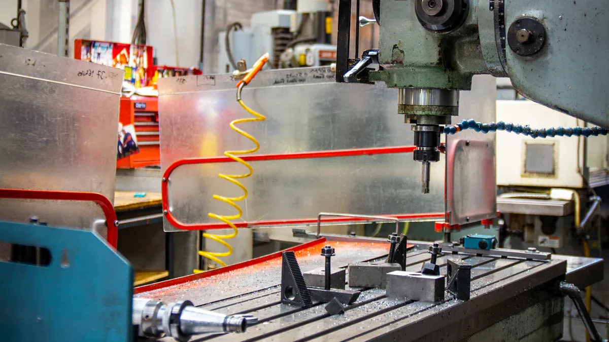
Preparing the PCB Surface
Preparing the surface of a PCB is a critical step in ensuring the success of vacuum deposition coating. A clean and well-prepared surface promotes better adhesion and uniformity of the protective layer. The preparation process involves several precise steps:
Cleaning the Panels: The panels undergo thorough cleaning to eliminate contaminants like dust, grease, or residues.
Application of Solder Mask: An epoxy solder mask ink is applied to both sides of the PCB to define the areas requiring protection.
UV Light Exposure: The boards are exposed to UV light through a solder mask photo film, hardening the covered portions.
Removal of Unhardened Portions: Unhardened areas are removed, leaving the desired pattern intact.
Curing the Solder Mask: The PCB is placed in an oven to cure the solder mask, ensuring durability.
Surface Finish Application: A chemical plating process applies gold or silver to enhance solderability. Hot air leveling ensures uniform pads for assembly.
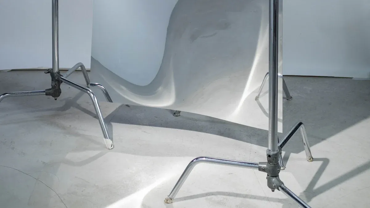
These steps create a pristine surface, ready for the application of parylene coating or other vacuum deposition techniques.
Vacuum Chamber Setup
The vacuum chamber setup is essential for achieving the controlled environment required for vacuum deposition coating. Technicians begin by ensuring the chamber is free from contaminants. They then load the prepared PCBs onto specialized fixtures designed to hold them securely during the process. The chamber is sealed, and air is evacuated to create a low-pressure environment. This vacuum minimizes impurities and enables precise control over the deposition process. Sensors and monitoring systems ensure optimal conditions, such as temperature and pressure, are maintained throughout the procedure.
Deposition of Protective Layers
The deposition phase involves applying the protective layer, such as parylene, onto the PCB surface. In the case of parylene coating, the process begins with the vaporization of parylene dimer. The vaporized material undergoes pyrolysis, breaking it into reactive monomers. These monomers then polymerize upon contact with the PCB, forming a uniform, pinhole-free coating. This method ensures comprehensive coverage, even on intricate geometries and sharp edges. The resulting layer provides exceptional moisture resistance, chemical stability, and electrical insulation. Once the deposition is complete, the chamber is vented, and the coated PCBs are carefully removed for inspection.
Note: Proper handling during this stage is crucial to prevent damage to the newly applied coating.
Post-Coating Inspection and Testing
Post-coating inspection and testing ensure the quality and reliability of vacuum deposition coating applied to PCBs. These processes verify that the protective layer meets the required standards and performs as intended in various applications.
Technicians employ several methods to evaluate the coating’s uniformity and adhesion. Contact angle measurements are a common technique. This method involves placing a drop of bio-inert liquid on the coated surface and observing how it interacts with the material. The way the liquid beads or spreads provides insights into the surface properties. Multiple measurements across the PCB surface can reveal inconsistencies in the coating application, ensuring comprehensive coverage.
Proper cleaning of the substrate before coating plays a vital role in achieving high-quality results. Residual contaminants can compromise adhesion and uniformity. To enhance bonding, thin seed or primer layers are often applied before the main coating process. These layers improve the overall durability and performance of the protective film.
Post-coating inspection also includes visual and microscopic examinations. These methods detect defects such as pinholes, cracks, or uneven thickness. Advanced techniques like X-ray fluorescence (XRF) analysis may be used to assess the coating’s composition and thickness. Electrical testing ensures that the coating provides adequate insulation and does not interfere with the PCB’s functionality.
Tip: Regular calibration of testing equipment ensures accurate and reliable results during the inspection process.
By combining these inspection and testing methods, manufacturers can guarantee that the vacuum deposition coating meets industry standards. This step is crucial for ensuring the long-term reliability and performance of PCBs in demanding environments.
Industry Use Cases for Vacuum Deposition Coating
Aerospace and Defense
Vacuum deposition coating plays a pivotal role in the aerospace and defense sectors, where components must endure extreme conditions and high speeds. This technology enhances the durability and performance of critical parts by providing wear resistance and protection against erosion. For example, physical vapor deposition (PVD) coatings safeguard aircraft components from oxidation, ensuring their reliability and safety during operation. These coatings also improve the longevity of parts exposed to harsh environments, such as jet engines and turbine blades. By minimizing wear and tear, vacuum deposition coating contributes to the overall safety and efficiency of aerospace systems.
Automotive Electronics
In the automotive industry, vacuum deposition coating enhances the performance and reliability of electronic components. This technology prevents corrosion and rust, which are common issues in automotive environments. It also improves the durability of parts like steering column components, exhaust gaskets, and brake clips. Additionally, vacuum coatings reduce problems such as screeching brakes, ensuring a smoother driving experience. These benefits make vacuum deposition coating an essential solution for modern automotive electronics, where durability and performance are critical.
Medical Devices
Vacuum deposition coating is indispensable in the medical field, where precision and reliability are paramount. This technology applies a thin protective layer, typically ranging from 0.25 to 10 microns, to medical devices. The coating ensures uniformity, even on hard-to-reach surfaces, which is crucial for maintaining device efficiency. For instance, bio-inert and hydrophilic coatings enhance the performance of devices like catheters by improving lubricity and reducing friction. These features increase patient comfort and minimize irritation during use. Vacuum deposition coating also provides a protective barrier that maintains the integrity of medical devices in demanding environments, ensuring their long-term functionality.
Consumer Electronics
Vacuum deposition coating has become a cornerstone in the development of modern consumer electronics. This advanced technology enhances both the functionality and aesthetics of devices, ensuring they meet the high expectations of today’s users. Its applications span a wide range of products, providing tailored solutions for durability, protection, and visual appeal.
Handheld electronic devices benefit significantly from vacuum deposition coating. UV clear coats applied to these devices offer exceptional scratch resistance, preserving their sleek appearance and extending their lifespan. This feature enhances the user experience by maintaining the device’s pristine condition over time.
Plastic enclosures in consumer electronics utilize conductive coatings to shield against electromagnetic interference (EMI) and radio frequency interference (RFI). This protection ensures the seamless operation of internal components, even in environments with high electromagnetic activity.
Decorative coatings elevate the aesthetic appeal of devices while simultaneously providing a protective barrier. These coatings add a premium finish to products, making them more attractive to consumers without compromising durability.
The versatility of vacuum deposition coating makes it indispensable in the consumer electronics industry. It not only safeguards the internal components of devices but also enhances their external features, ensuring a perfect balance between performance and design. This dual functionality supports the growing demand for reliable and visually appealing electronics.
Industrial Applications in Harsh Environments
Industrial environments often expose equipment and components to extreme conditions, including high temperatures, friction, and corrosive substances. Vacuum deposition coating addresses these challenges by providing robust protection that ensures long-term reliability and performance.
This process involves applying thin layers of material under vacuum conditions, enhancing resistance to wear, heat, and mechanical stress. Industries such as automotive, aerospace, and medical rely on this technology to maintain the integrity of their equipment. For example:
In the automotive industry, components like engine parts and exhaust systems face high temperatures and corrosive environments. Durable coatings protect these parts, ensuring optimal performance and longevity.
The aerospace sector benefits from coatings that withstand rapid temperature changes and mechanical stresses. These coatings enhance the reliability of critical components, such as turbine blades and structural parts.
In the medical field, instruments endure frequent sterilization and use. Vacuum deposition coatings maintain their integrity, ensuring consistent performance and patient safety.
Challenge | Solution |
|---|---|
High capital cost | PVD technology can replace conventional wet processes, providing superior coating performance. |
Special operating considerations | PVD systems can operate at high temperatures and vacuums, requiring tailored operational protocols. |
Vacuum deposition coating proves essential in harsh industrial environments. Its ability to enhance durability and functionality ensures that equipment operates efficiently, even under the most demanding conditions.
Vacuum deposition coating has proven to be an essential solution for protecting PCBs in modern electronics. Its ability to enhance durability, waterproofing, and chemical resistance ensures reliable performance across various industries. By extending the lifespan of PCBs, this technology minimizes the need for frequent repairs or replacements, reducing long-term production costs. The uniformity of the coating also decreases material waste, making it a sustainable choice for PCB assembly.
This advanced coating method offers unmatched reliability and versatility. Businesses seeking to improve the performance and longevity of their PCBs should consider adopting vacuum deposition coating as a key part of their manufacturing process.
FAQ
What makes vacuum deposition coating superior to traditional methods?
Vacuum deposition coating ensures precision and uniformity by operating in a controlled vacuum environment. This process minimizes contamination and enhances adhesion, making it more reliable than traditional methods. It also offers superior durability, moisture resistance, and chemical protection, which are essential for safeguarding PCBs in demanding applications.
Can vacuum deposition coating be applied to all PCB designs?
Yes, vacuum deposition coating can adapt to various PCB designs, including intricate geometries and sharp edges. Techniques like parylene coating ensure comprehensive coverage, even on complex surfaces. This versatility makes it suitable for a wide range of industries, from aerospace to consumer electronics.
How does vacuum deposition coating improve PCB performance?
Vacuum deposition coating enhances PCB performance by improving thermal management and electrical conductivity. It creates a uniform layer that dissipates heat efficiently and reduces surface defects. This ensures optimal functionality, especially in high-frequency circuits, while also providing insulation to prevent electrical interference or short circuits.
Is vacuum deposition coating environmentally friendly?
Yes, vacuum deposition coating is an environmentally friendly option. The process generates minimal hazardous waste compared to traditional methods. Its precise application reduces material waste, making it a sustainable choice for industries aiming to minimize their environmental impact.
What industries benefit the most from vacuum deposition coating?
Industries like aerospace, automotive, medical devices, and consumer electronics benefit significantly. For example, aerospace relies on it for wear resistance, while medical devices use it for bio-inert coatings. Its versatility ensures reliable performance across diverse applications, even in harsh environments.
Tip: Consult industry experts to determine the best vacuum deposition technique for your specific application.